
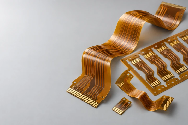
Flexible Printed Circuits
Flexible PCB Manufacturing & Fabrication
Custom flex circuits for compact connections and demanding assembly layouts. Explore material choices, layer structures, and our standard and advanced manufacturing capabilities.
Get Your Flex PCB QuoteFlexible Circuits for Modern Electronics
A flexible circuit brings the connection into the shape of your product. Plan the routing, installation bends, and connector interfaces together, whether the project is a compact instrument, a wearable assembly, or an industrial module.
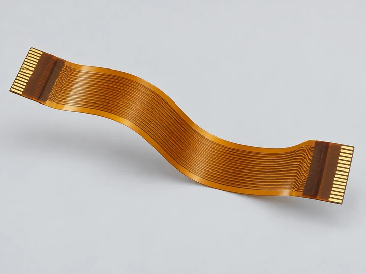
Flexible PCB Advantages
Connections That Fit Your Product
Fit Compact Spaces
Route connections between circuit sections arranged on different planes inside an enclosure.
Reduce Separate Wiring
Integrate selected electrical connections into one defined circuit pattern, reducing the number of individual wiring parts where the design allows.
Plan Installation Bends
Fold a static flex circuit into its intended position with a stack-up and bend radius chosen for the assembly.
Design for Defined Movement
Repeated movement needs an appropriate construction and an agreed validation plan. Specify bend geometry and required cycles early.
Material Comparison
Adhesive & Adhesiveless Polyimide Options
Compare the constructions listed in our capability sheet and specify the exact laminate, copper, coverlay, and reinforcement.
| Item | Adhesive Polyimide | Adhesiveless Polyimide |
|---|---|---|
| Listed laminate families | Shengyi SF305 | Panasonic R-F775; Taiflex MHK; DuPont Pyralux AP |
| Standard PI thickness options | 0.5 / 1 / 2 mil | Grade-dependent options from 1 to 3 mil |
| Standard copper options | 0.33 / 0.5 / 1 oz | Grade-dependent options of 0.33 / 0.5 / 1 oz |
| Advanced options in the sheet | No separate advanced entry | R-F775: PI 3 mil, Cu 2 oz; Pyralux AP: PI 4 mil, Cu 2 oz |
| Selection criteria | Confirm the complete stack-up, adhesive system, assembly conditions, electrical requirements, and bending duty. | |
View full laminate, coverlay, adhesive, and stiffener options
| Parameter | Standard | Advanced | Conditions |
|---|---|---|---|
| Adhesive FCCL: Shengyi SF305 | PI: 0.5 / 1 / 2 mil; Cu: 0.33 / 0.5 / 1 oz | — | — |
| Adhesiveless FCCL: Panasonic R-F775 | PI: 1 / 2 / 3 mil; Cu: 0.5 / 1 oz | PI: 3 mil; Cu: 2 oz | — |
| Adhesiveless FCCL: Taiflex MHK | PI: 1 / 2 mil; Cu: 0.33 / 0.5 / 1 oz | — | — |
| Adhesiveless FCCL: DuPont Pyralux AP | PI: 1 / 2 / 3 mil; Cu: 0.5 / 1 oz | PI: 4 mil; Cu: 2 oz | — |
| Coverlay: Shengyi SF305C | 0515 / 0525 / 1025 / 2030 | — | — |
| Coverlay: Taiflex FHK | 1025 / 2035 | — | — |
| Adhesive: Taiflex BT | 10 / 25 / 40 μm | — | — |
| PI stiffener: Taiflex MHK | PI: 3 / 5 / 7 / 9 mil | — | — |
| 3M adhesive products | 9077 / 6677 / 9058 | — | — |
Circuit Structures
Single-Layer, Double-Layer & Multilayer Flex PCBs
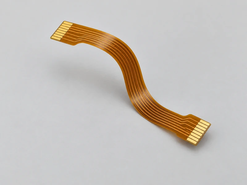
Single-Layer Flex
A single conductive layer for comparatively simple interconnections.
- One copper routing layer on a flexible construction.
- Define contact access and exposed connection areas.
- Specify reinforcement at connector interfaces.
- Coordinate bend location with the mechanical assembly.
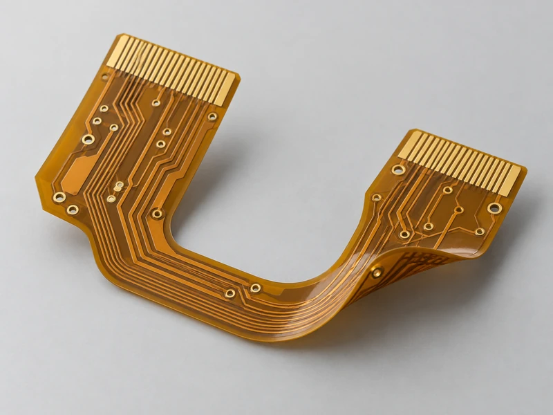
Double-Layer Flex
Two conductive layers provide additional routing paths.
- Define interlayer connections in the fabrication data.
- Review plated-hole locations near bending regions.
- Specify coverlay openings on each applicable side.
- Evaluate the construction against installation or movement.
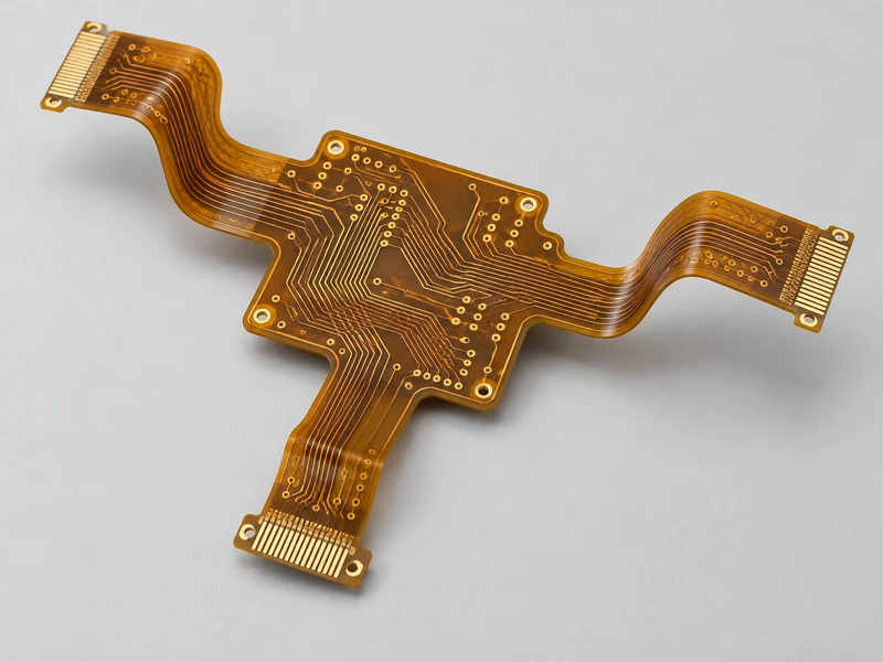
Multilayer Flex
Multiple conductive layers support more involved routing requirements.
- Standard layer range: 1–4; advanced range: 5–8.
- Provide a complete layer-by-layer stack-up.
- Review thickness, interconnections, and impedance requirements.
- Confirm the bending plan for the selected construction.
Process Technology
Flexible PCB Manufacturing Capabilities
Standard and advanced process ranges from our 2025 capability sheet. Confirm combinations and project-specific conditions during engineering review.
| Feature | Capability |
|---|---|
| Layers | 1–4 standard; 5–8 advanced |
| Thickness without stiffeners | 0.05–0.5 mm standard; 0.5–0.8 mm advanced |
| Single / double-layer tolerance | ±0.05 mm standard; ±0.03 mm advanced, with thickness conditions |
| Multilayer tolerance, 0.3–0.8 mm | ±0.1 mm standard; ±10% advanced |
| Maximum size | 9 × 14 in standard; 9 × 23 in advanced (PI ≥1 mil) |
| Minimum size without bridge | 5 × 10 mm standard; 4 × 8 mm advanced |
| Impedance, single-ended | ±5 Ω / ±10% standard; ±3 Ω / ±8% advanced (threshold: 50 Ω) |
| Impedance, differential | ±5 Ω / ±10% standard; ±4 Ω / ±8% advanced (threshold: 50 Ω) |
| Feature | Capability |
|---|---|
| Mechanical drill | 6 mil standard; 4 mil advanced |
| Inner trace / space, 12/18 μm Cu | 3.0 / 3.2 mil standard; 2.8 / 2.7 mil advanced; loop limits differ |
| Outer trace / space, 18 μm Cu | 3 / 3.2 mil standard; 2.8 / 2.7 mil advanced; loop limits differ |
| Maximum finished outer copper | 3 oz standard; 5 oz advanced |
| Coverlay bridge | 8 mil |
| Mask / silkscreen | Green mask; white or yellow silkscreen |
| Surface finishes | ENIG, ENEPIG, HASL, electrolytic nickel gold, soft/hard gold, immersion silver, OSP; immersion tin advanced |
| Outline accuracy | Laser ±0.05 mm; punch ±0.05 to ±0.15 mm |
Full standard / advanced board and interconnection specifications
| Parameter | Standard | Advanced | Conditions |
|---|---|---|---|
| Layer count | 1–4 | 5–8 | — |
| Board thickness, excluding stiffeners | 0.05–0.5 mm | 0.5–0.8 mm | — |
| Single-layer thickness tolerance | ±0.05 mm | ±0.03 mm | Excluding stiffeners |
| Double-layer thickness tolerance (≤0.3 mm) | ±0.05 mm | ±0.03 mm | Excluding stiffeners |
| Multilayer thickness tolerance (<0.3 mm) | ±0.05 mm | ±0.03 mm | Excluding stiffeners |
| Multilayer thickness tolerance (0.3–0.8 mm) | ±0.1 mm | ±10% | Excluding stiffeners |
| Thickness tolerance including PI stiffener | ±0.05 mm | ±10% | — |
| Thickness tolerance including FR4 stiffener | ±0.1 mm | ±10% | — |
| Minimum outline, without bridge | 5 × 10 mm | 4 × 8 mm | — |
| Minimum outline, with bridge | 10 × 10 mm | 8 × 8 mm | — |
| Maximum board size | 9 × 14 in | 9 × 23 in | Advanced: PI ≥1 mil |
| Single-ended impedance tolerance | ±5 Ω (≤50 Ω); ±10% (>50 Ω) | ±3 Ω (≤50 Ω); ±8% (>50 Ω) | — |
| Differential impedance tolerance | ±5 Ω (≤50 Ω); ±10% (>50 Ω) | ±4 Ω (≤50 Ω); ±8% (>50 Ω) | — |
| Minimum coverlay bridge | 8 mil | — | — |
| Minimum mechanical drill | 6 mil | 4 mil | — |
| Via-to-conductor distance: <4 layers | 6 mil | 5 mil | — |
| Via-to-conductor distance: 4–6 layers | 8 mil | 7 mil | — |
| Via-to-conductor distance: 7–8 layers | 12 mil | 10 mil | — |
| Laser outline accuracy | ±0.05 mm | — | — |
| Punch outline accuracy | ±0.05 to ±0.15 mm | — | — |
Trace / space by copper thickness, including loop-line limits
| Parameter | Standard | Advanced | Conditions |
|---|---|---|---|
| Inner, 12/18 μm copper | 3.0 / 3.2 mil; loops 6.0 / 6.2 mil | 2.8 / 2.7 mil; loops 5 / 5.2 mil | — |
| Inner, 35 μm copper | 4.0 / 4.0 mil; loops 8.0 / 8.0 mil | 3.5 / 3.5 mil; loops 7 / 7 mil | — |
| Inner, 70 μm copper | 6 / 6.5 mil; loops 10 / 10.5 mil | 5 / 6 mil; loops 9 / 9.5 mil | — |
| Maximum inner-layer copper | 2 oz | 3 oz | — |
| Outer, 18 μm copper | 3 / 3.2 mil; loops 6 / 6 mil | 2.8 / 2.7 mil; loops 5.5 / 5.5 mil | — |
| Outer, 35 μm copper | 4 / 4.5 mil; loops 8 / 8.5 mil | 3.5 / 3.5 mil; loops 7.5 / 7.5 mil | — |
| Outer, 70 μm copper | 6 / 7 mil; loops 10 / 11 mil | 5.5 / 8.5 mil; loops 9.5 / 10.0 mil | Values retained as listed in the capability sheet |
| Outer, 105 μm copper | 10 / 13 mil; loops 12 / 15 mil | 9.5 / 12.5 mil; loops 11.5 / 14.5 mil | — |
| Maximum finished outer copper | 3 oz | 5 oz | — |
Surface finishes, plating thicknesses, mask and silkscreen
| Parameter | Standard | Advanced | Conditions |
|---|---|---|---|
| Surface finishes | HASL, ENIG, ENEPIG, electrolytic nickel gold, soft gold, hard gold, immersion silver, OSP | Immersion tin | — |
| Mixed finishes | ENIG + OSP; ENIG + G/F | — | — |
| ENIG gold thickness | 0.05–0.10 μm | — | — |
| ENIG nickel thickness | 3–6 μm | — | — |
| ENEPIG gold thickness | 0.05–0.10 μm | — | — |
| ENEPIG palladium thickness | 0.05–0.15 μm | — | — |
| ENEPIG nickel thickness | 3–6 μm | — | — |
| Electrolytic nickel thickness | 3–6 μm | — | — |
| Electrolytic gold thickness | 0.05–0.10 μm | — | — |
| OSP thickness | 0.1–0.3 μm | — | — |
| Immersion silver thickness | 0.2–0.4 μm | — | — |
| Solder mask | Green | — | — |
| Silkscreen | White or yellow | — | — |
| Minimum solder dam, base copper ≤1 oz | 4 mil (green); 8 mil on large copper areas | — | — |
Bend-radius guidance and dynamic-flex conditions
| Construction | Listed bend-radius range |
|---|---|
| Single layer | 3–6 × thickness |
| Double layer | 6–10 × thickness |
| Multilayer | 10–15 × thickness |
| Dynamic, single layer only | 20–40 × thickness |
These are review ranges, not universal bend-life guarantees. Define bend axis, angle, movement, and required cycles for the actual stack-up.
A dash in the detailed tables means no separate advanced value is listed. Capabilities are not assumed to be simultaneously achievable. The 70 μm outer-copper advanced width / spacing value is retained as 5.5 / 8.5 mil from the source sheet.
Product Gallery
Flexible PCB Product Concepts
Explore possible circuit forms for your next assembly. Send your drawing to confirm the actual construction and specifications.
Flexible Interconnect Tail
Parallel routing and a shaped connector tail, illustrated for compact internal connections.
Discuss a Similar Design →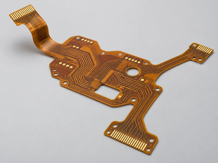
Branched Flexible Circuit
A shaped circuit with multiple connection areas, illustrated for a more complex assembly layout.
Discuss a Similar Design →Flexible Circuit Panel & Curved Tails
An illustration of circuit shapes and panel arrangements to discuss during design review.
Discuss a Similar Design →About MV Circuit
Your PCB Manufacturing & Assembly Partner
MV Circuit’s Advantages
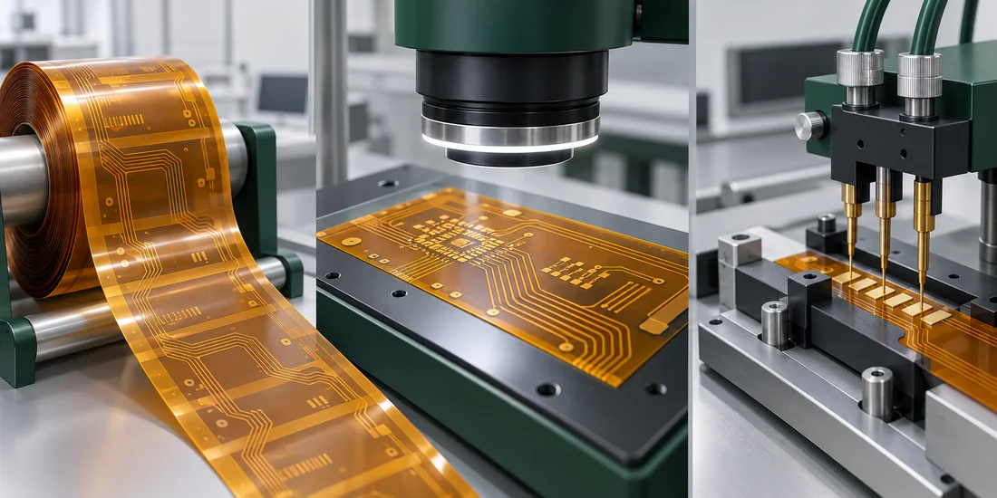
MV Circuit provides PCB fabrication and assembly services for customers across Europe, North America, and Asia. With over 18 years of PCBA manufacturing experience, we support customized flexible, rigid-flex, and rigid PCB projects, from prototypes to production.
Our one-stop service covers PCB fabrication, component sourcing, SMT, testing, and assembly. Full CAM review before manufacturing, strict incoming material inspection, and traceable production records help us manage quality throughout the process. A dedicated project manager and 24/7 sales and engineering support keep your project moving with timely communication and proactive weekly WIP updates.
Watch Flexible PCB Manufacturing
See the manufacturing topic in your PCBMay official channel video. Include fabrication data, drill files, the stack-up, and bend requirements with your inquiry.
- Fabrication files: RS-274-D / RS-274-X Gerber.
- Drill data: Excellon format.
- Mechanical details: outline, reinforcement, and contact interfaces.
Quality Planning
Testing & Inspection
Define the acceptance requirements for the actual circuit and its intended application.
Visual & Surface Review
Specify coverlay alignment, contact areas, surface condition, and the agreed inspection criteria.
Electrical Verification
Define continuity, isolation, and any additional application-specific electrical checks.
Mechanical Acceptance
Confirm outline, thickness, reinforcement, and connector fit. Bend-life validation requires an agreed test plan.
Start Your Project
Request Flexible PCB Fabrication or Assembly
Send your Gerber and Excellon files, stack-up, mechanical drawing, quantity, and required delivery date. Include reinforcement, bend conditions, and assembly files where applicable.
Get Your QuoteEmail: info@mv-circuit.com
Common Questions
Flexible PCB FAQ
What is the difference between static and dynamic flex?
Static flex is bent into position during installation. Dynamic flex experiences repeated movement during operation and needs a construction designed and validated for that duty.
When does a flexible PCB need stiffeners?
Stiffeners can reinforce connector interfaces and component mounting areas. Their material, thickness, and placement should be specified in the mechanical drawing.
What should I include with my inquiry?
Provide fabrication files, layer construction, mechanical drawings, stiffener details, quantity, and bending requirements. Include assembly files if components are required.
Which materials should I specify for a flexible PCB?
Specify the required laminate, copper, adhesive system, coverlay, and operating conditions. The final material combination should be reviewed against assembly temperature and bending requirements.
What bend radius should I use?
The capability sheet lists 3–6 times thickness for single-layer flex, 6–10 times for double-layer, and 10–15 times for multilayer. Dynamic single-layer guidance is 20–40 times thickness. Final radius and cycle validation depend on the actual stack-up.
What is coverlay and where are openings needed?
Coverlay protects the flexible circuit while openings expose connection or assembly areas. Define the openings and required clearances in your fabrication data.
Can components be mounted on a flexible PCB?
Yes, provided the mounting regions and assembly support are designed for the components and process. Keep the intended bending areas separate from component attachment regions.
How should I specify a ZIF connector tail?
Provide the connector part number or interface drawing, contact pitch, exposed contact geometry, insertion direction, and required finished tail thickness.
How can a flexible PCB replace a cable harness?
A flex circuit can integrate selected interconnections into a defined circuit pattern. Suitability depends on current, signal requirements, available space, movement, and termination design.
What affects flexible PCB cost and lead time?
Material selection, layer construction, outline complexity, stiffeners, quantity, assembly needs, and inspection requirements affect the quote and schedule. These are confirmed after file review.
Customer Feedback
What Our Customers Say
“Their PCB manufacturing capabilities are top-notch, and the communication throughout the process is seamless. We highly recommend them for any PCB needs in the future.”
Sarah L. · Germany
Existing feedback about MV Circuit’s overall PCB service. View the original feedback.