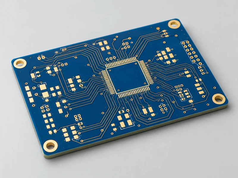
4-Layer PCBs
A practical construction for compact controllers and general electronics.
Coordinate signal layers with suitable ground and power references.

CONNECTED LAYERS • COORDINATED MANUFACTURING
Bring routing density, reference planes, and power distribution together in a stack-up built around your design. MV Circuit supports multilayer PCB projects from prototypes to production.
MULTILAYER CONSTRUCTION
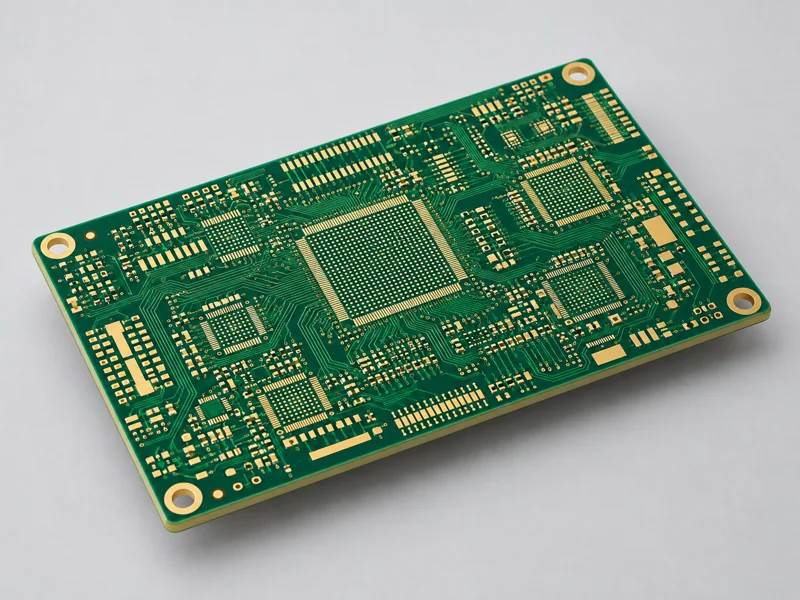
Multilayer PCBs combine signal and power conductors across internal and external layers. Their compact structure supports complex interconnections while allowing designers to assign reference planes and manage routing space.
The benefits depend on the complete design: layer order, return paths, dielectric properties, copper balance, and via transitions. Layer count should follow your electrical and mechanical requirements.
MV Circuit reviews fabrication files and stack-up requirements before production. We coordinate materials, lamination, drilling, plating, solder mask, surface finish, and the agreed inspection plan.
LAYER OPTIONS
A practical construction for compact controllers and general electronics.
Coordinate signal layers with suitable ground and power references.
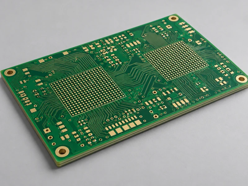
Additional routing space and reference-plane options for more complex designs.
Plan signal transitions, power distribution, and copper balance together.
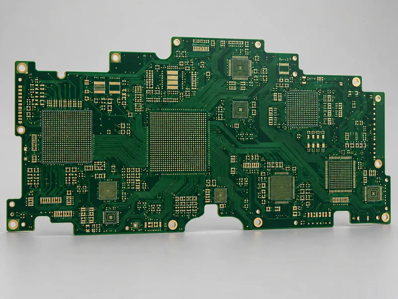
Dense interconnections for demanding computing, communication, and industrial systems.
Confirm the full stack-up, via strategy, registration, and inspection scope.
STACK-UP ENGINEERING
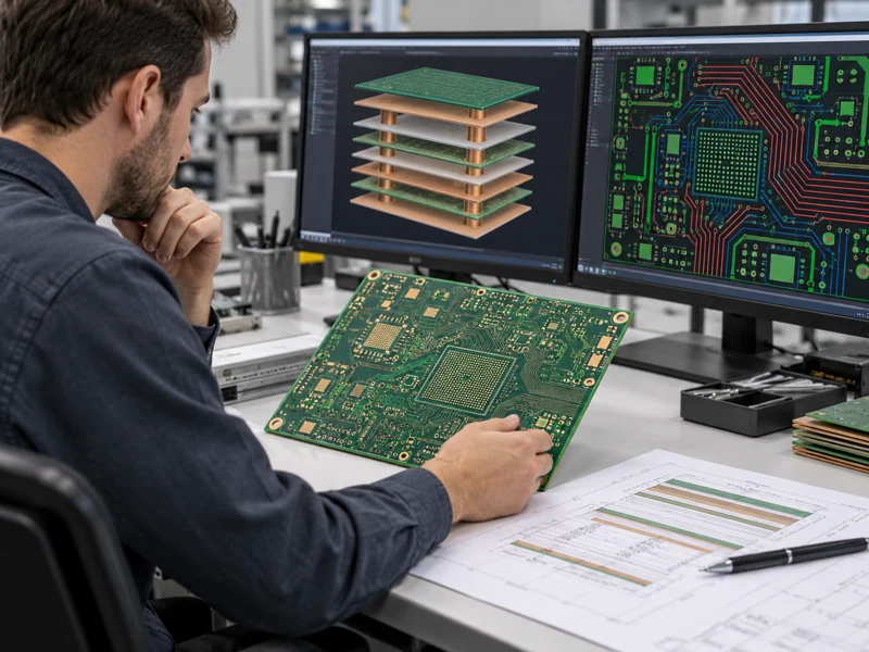
Specify layer order, signal routing regions, reference planes, and intended return paths. Review layer changes alongside the electrical design.
Use the approved laminate grade and construction. Coordinate dielectric properties, finished thickness, thermal requirements, and material availability.
Provide impedance targets, tolerances, trace layers, and reference planes. Agree geometry adjustments and coupon requirements before release.
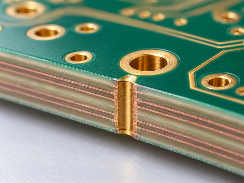
Review copper distribution, drill spans, via filling, and lamination sequence. Identify asymmetric constructions and special tolerances early.
FABRICATION REVIEW
Use this overview to prepare an inquiry. Final limits are confirmed for the actual stack-up; independent maximum values do not necessarily apply together.
| Feature | Manufacturing Scope | Project Review |
|---|---|---|
| Layer count | 4-layer, 6-layer, 8-layer and higher-layer builds | Published multilayer service up to 40 layers; confirm the complete construction. |
| Base materials | Specified FR-4 and high-Tg FR-4 | Low-loss, specialty laminates and hybrid builds by engineering review. |
| Copper requirement | Define copper weight layer by layer | Distinguish starting foil from finished copper on plated outer layers. |
| Board thickness | Finished thickness to the approved drawing | Core/prepreg construction, tolerances, aspect ratios, and panel stability reviewed together. |
| Line width and spacing | Published fine-line reference around 3/3 mil | Actual limits depend on copper thickness, layer type, material, and geometry. |
| Interconnections | Plated through-holes and non-plated features | Blind/buried vias and via-in-pad filling reviewed for the selected build. |
| Controlled impedance | Single-ended and differential requirements by design | Agree stack-up, geometry, tolerances, coupons, and measurement scope. |
| Surface finish | ENIG, OSP, lead-free HASL, immersion tin or silver | Selective and specialty finishes assessed against assembly and contact requirements. |
| Inspection and acceptance | Electrical continuity/isolation and agreed visual inspection | Specify IPC class, coupon/cross-section scope, documentation, and special acceptance needs. |
MATERIALS & LAMINATION
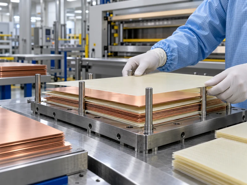
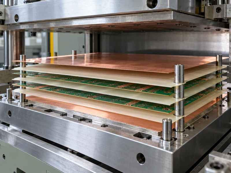
Multilayer construction brings patterned cores, prepreg, and copper foil together under a defined lamination process. Material identity, layer alignment, and the approved press construction matter throughout the build.
Specify the laminate grade and relevant electrical and thermal requirements. Review resin fill, copper distribution, dielectric spacing, and the effect of subsequent drilling and plating.
For high-speed or mixed-material designs, coordinate material properties and fabrication requirements before placing the order.
MANUFACTURING WORKFLOW
01
Align layer order, materials, impedance targets, copper weights, drill spans, and acceptance requirements.
02
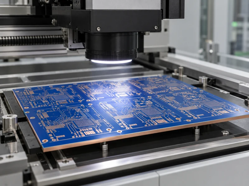
Form the inner conductor patterns and inspect them before they become buried inside the board.
03
Register the approved cores, prepreg, and foil, then bond the construction using the agreed process.
04
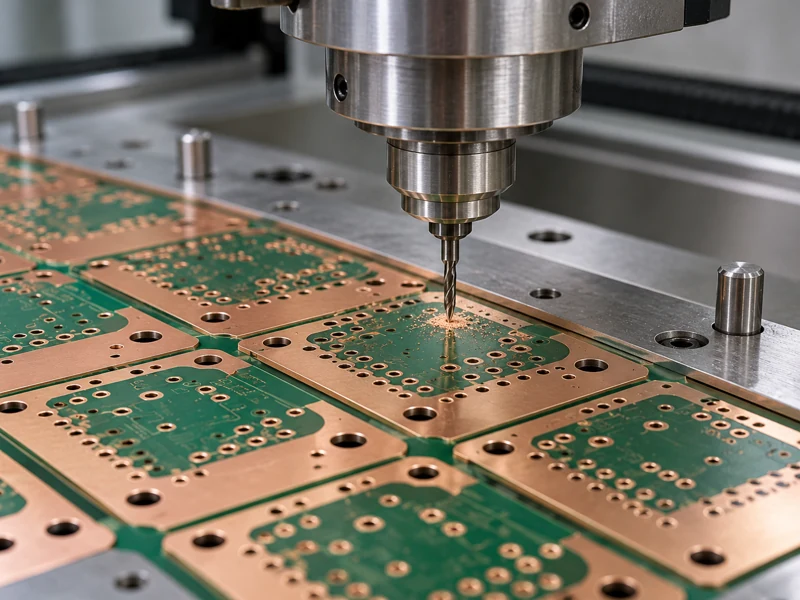
Create the required holes, prepare the hole walls, and establish plated connections between layers.
05
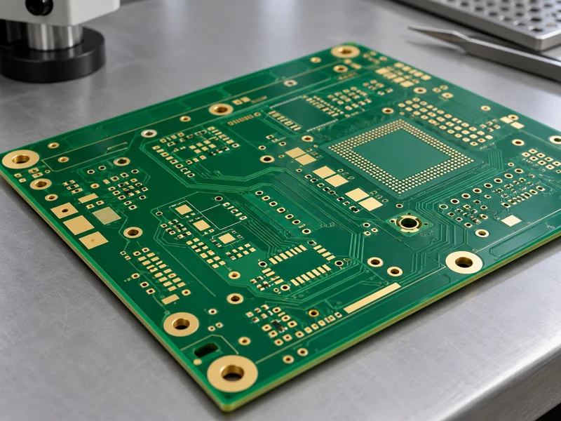
Complete outer conductor formation, solder mask, markings, and the specified finish.

06
Verify net connectivity and isolation, complete the agreed inspection, and protect boards for shipment.
TESTING & INSPECTION
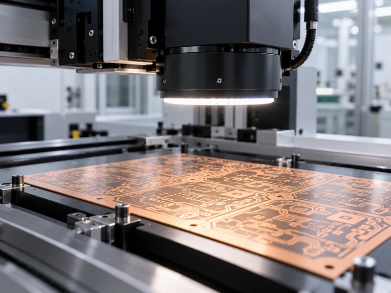
Inspect accessible inner-layer conductors for pattern defects against approved artwork before lamination.
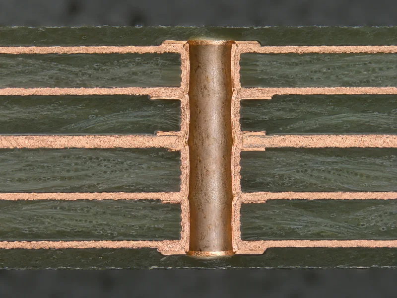
Agree registration, finished thickness, plated-hole quality, and sample or coupon examination requirements.
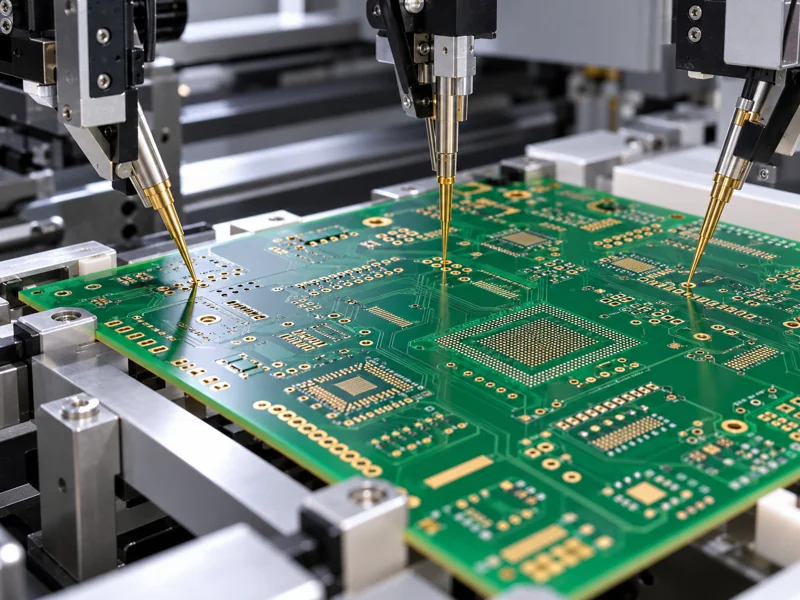
Test bare-board nets for opens and shorts. Impedance and other special measurements follow the agreed acceptance plan.
APPLICATIONS
Automation, embedded controllers, sensor interfaces, and instrumentation.
Network interfaces, connected devices, RF subsystems, and data communication electronics.
Processor boards, memory interfaces, and space-constrained embedded systems.
Control and power distribution layers coordinated with analog and digital routing.
MV CIRCUIT
MV Circuit provides PCB fabrication and assembly support for customers across Europe, North America, and Asia. We bring fabrication drawings, material requirements, layer connections, and project communication together before production.
With over 18 years of PCBA manufacturing experience, our team supports prototypes and production orders. CAM and DFM review, material inspection, and traceable production records help coordinate the build.
A dedicated project contact helps resolve technical questions and production updates. Component sourcing and assembly support allow you to plan beyond the bare board.

MANUFACTURING VIDEO
Watch the production overview from our official manufacturing channel. Discuss the layer structure and inspection needs of your own project with MV Circuit.
START YOUR PROJECT
Send fabrication and drill files, layer stack-up, material grade, copper weights, board thickness, surface finish, quantities, and delivery target. Include impedance, via filling, special tolerances, and acceptance requirements.
Send Your Multilayer PCB Inquiry
Email: info@mv-circuit.com
COMMON QUESTIONS
A multilayer PCB contains more than two copper layers separated by insulating material and bonded into one board. Plated interconnections link selected layers. The fabrication drawing defines the layer order, materials, thicknesses, copper weights, and connection requirements.
Layer count depends on routing density, reference-plane needs, power distribution, board size, and signal requirements. Start with the electrical and mechanical design, then review a manufacturable stack-up. More layers alone do not guarantee better signal integrity.
Our published multilayer service includes boards up to 40 layers. Availability depends on board dimensions, material, thickness, via construction, and acceptance requirements. Submit the complete stack-up for confirmation rather than combining independent maximum capabilities.
Identify each copper layer and its function, starting or finished copper thickness, core and prepreg construction, material grade, dielectric thickness, and target finished board thickness. Include impedance requirements and any permitted adjustments.
Provide target impedance, tolerance, trace type, relevant layers, and the intended reference planes. The fabricator reviews geometry against actual material data and the manufacturing stack-up. Agree coupon design and measurement requirements before production.
FR-4 and high-Tg FR-4 are common choices. Low-loss and specialty laminates or hybrid constructions can be reviewed for demanding applications. Specify the exact grade and relevant thermal, electrical, and qualification requirements; a generic material name is insufficient for substitution.
Blind, buried, and via-in-pad structures can be assessed for your design. Layer connections, drill method, aspect ratio, filling, and sequential lamination affect manufacturability and cost. HDI microvias require a specifically agreed construction.
Options include ENIG, OSP, lead-free HASL, immersion tin or silver, with selective or other finishes by review. Choose according to component pitch, flatness, solderability, storage, contact wear, and assembly requirements.
Inspection can include inner-layer AOI, registration and dimensional checks, agreed cross-section analysis, and bare-board electrical continuity and isolation tests. Impedance testing follows the specified coupon and acceptance plan. Functional testing applies to assemblies under a separate test specification.
Send fabrication and drill files, a layer map and stack-up, board outline and dimensions, material grade, copper weights, surface finish, quantities, and delivery target. Add impedance, via filling, special tolerances, inspection requirements, and assembly data where relevant.
CUSTOMER FEEDBACK
“MV Circuit consistently delivers top-quality multilayer PCBs with precision and reliability. Their fast turnaround and professional support make them our go-to supplier.”John M. · USA
“We rely on MV Circuit for complex multilayer PCB designs. Their engineering expertise and strict quality control ensure our products meet the highest standards.”Anna L. · Italy
“MV Circuit provides durable, high-performance multilayer PCBs that withstand demanding environments. Their commitment to service and excellence has strengthened our long-term partnership.”David K. · UK