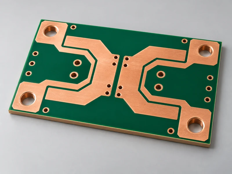
Double-Sided Power Boards
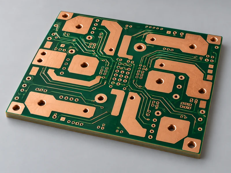
A direct construction for broad power routes on the two outer faces.
- Coordinate large terminal holes and pad areas.
- Specify finished surface copper and barrel plating.
- Review board outline and mounting requirements.

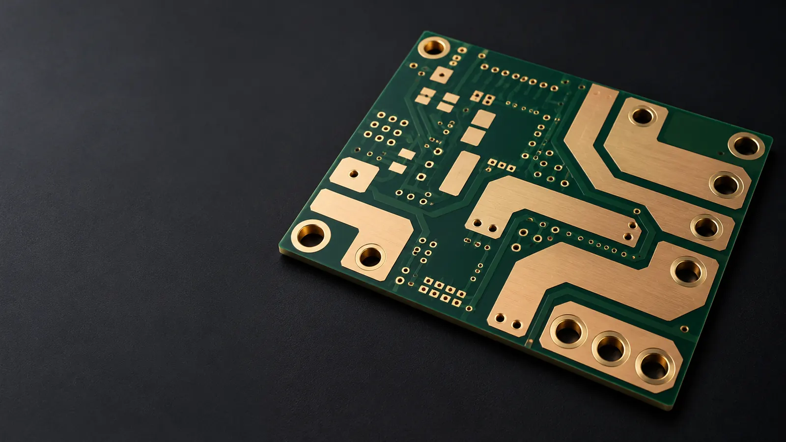
HIGH-CURRENT • POWER ELECTRONICS
Build a stronger path for power. MV Circuit helps turn your copper thickness, thermal requirements, and connection strategy into a manufacturable PCB specification.
POWER WITH PURPOSE
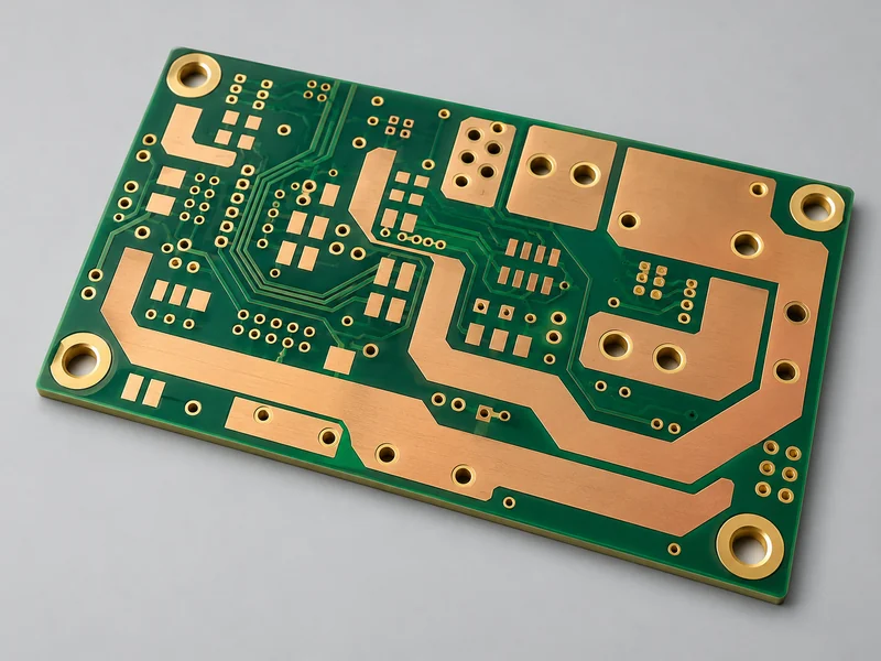
A heavy copper PCB uses thicker copper traces and planes to increase conductor cross-section. It can support power distribution and help spread heat, while keeping electrical interconnections within the circuit board.
For converters, charging equipment, and industrial controls, the benefit depends on the complete path: conductor width, layer transitions, terminal pads, plated holes, and cooling. Increasing copper weight alone does not establish a board current rating.
MV Circuit reviews your fabrication data and operating requirements before confirming the build. We coordinate the copper structure with dielectric spacing, etching, lamination, solder mask, and assembly.
DESIGN PRIORITIES
For a given width and path length, a thicker copper section reduces electrical resistance. Review the narrowest section of the complete path, including neck-downs, connectors, and layer changes.
Combine copper thickness with conductor area, thermal spreading, airflow, enclosure temperature, and heat removal. Validate the design under its intended continuous load and transient conditions.
Separate the needs of high-current paths and dense control signals. Copper weights, stack-up, and layout clearances should work together rather than forcing one geometry across every layer.
Heavier copper changes etching, resin fill, mask coverage, and soldering requirements. Early DFM review helps identify spacing or construction changes before tooling and production.
COPPER SELECTION
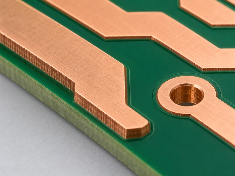
Start with your electrical and thermal needs, then agree the copper requirement for each layer. These nominal conversions help you prepare a fabrication drawing.
| Copper weight | Nominal thickness | Design discussion |
|---|---|---|
| 3 oz/ft² | ≈105 µm | A starting point for heavier conductors; confirm the finished layer requirement. |
| 4 oz/ft² | ≈140 µm | Review power-path width, etching clearance, and mask coverage. |
| 6 oz/ft² | ≈210 µm | Coordinate copper distribution, dielectric fill, and terminal geometry. |
| 10 oz/ft² | ≈350 µm | Evaluate the full thick-copper process route and assembly heat demand. |
| Higher copper weights | Project-specific | Send the stack-up and application for a dedicated feasibility assessment. |
Approximately 35 µm per oz/ft² is a nominal conversion, not a finished-board tolerance. Starting foil, outer-layer plating, and specified finished copper are different quantities. Agree acceptance limits and measurement locations before manufacture.
CONSTRUCTION OPTIONS
A direct construction for broad power routes on the two outer faces.
Distribute power across a defined multilayer stack-up while maintaining control and signal routing.
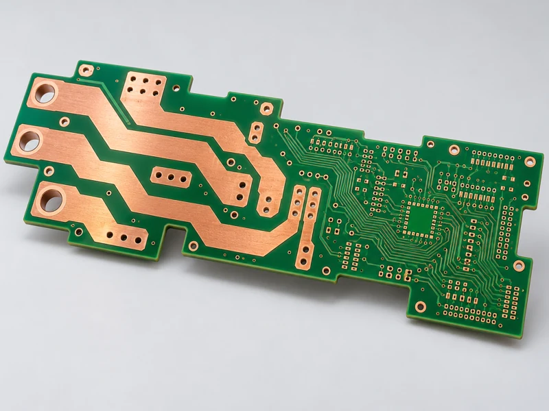
Use heavier power layers alongside thinner routing layers where the process and design allow.
FABRICATION REVIEW
Use these ranges to start an inquiry. Available limits depend on copper thickness, layer count, material, geometry, and the inspection plan; maximum values are not assumed to apply together.
| Feature | Standard / reference | Advanced / project review |
|---|---|---|
| Copper requirement | 0.5–4 oz copper options in the reference standard range | Heavier copper builds by engineering review; MV Circuit’s published fabrication offering includes heavy copper up to 60 oz. |
| Layer count | 1–20 layers | 22–40 layers subject to the approved copper structure and process. |
| Finished board thickness | 0.2–3.2 mm reference range | 3.4–10 mm reference range; confirm the complete stack-up. |
| Maximum board size | 500 × 600 mm reference format | Up to 1100 × 500 mm subject to copper weight and panel planning. |
| Base material | Specified FR-4 / high-Tg FR-4 grades | Specialty materials and hybrid constructions assessed for the application. |
| Surface finish | ENIG, OSP, lead-free HASL, immersion silver or tin | ENEPIG, selective or hard gold and combined finishes by review. |
| Solder mask | Green, black, blue, red, white and other requested colors | Mask coverage, thickness, openings and dams reviewed against the copper profile. |
| Hole / via construction | Plated and non-plated holes to the approved drawing | Specify barrel copper, slots, filling requirements, and inspection criteria separately. |
| Copper weight | Internal trace / space | External trace / space |
|---|---|---|
| 3 oz | 5 / 8 mil | 6 / 12 mil |
| 4 oz | 6 / 11 mil | 7.5 / 15 mil |
| 10 oz | 12 / 28 mil | 14 / 38 mil |
Line/space figures are starting references from our related manufacturing site. They require confirmation for the actual build and do not define voltage clearance or creepage. Higher copper weights need their own rules. Material availability, acceptance tolerances, panelization, and delivery are confirmed with the quotation.
PRODUCT GALLERY
Different power paths call for different board layouts. Share your current, connection, and enclosure requirements with our engineering team.
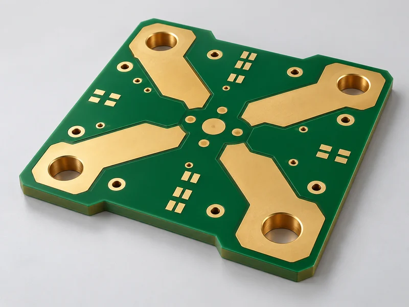
Broad conducting paths and substantial connection pads for distributing power between system terminals.
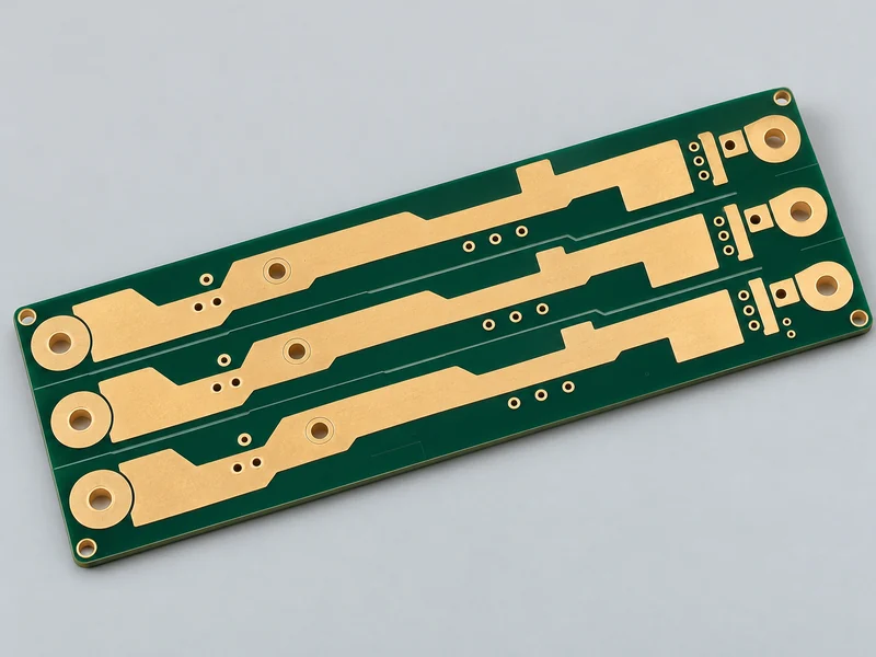
Coordinate multiple power channels, control routing, mounting holes, and the thermal interface.
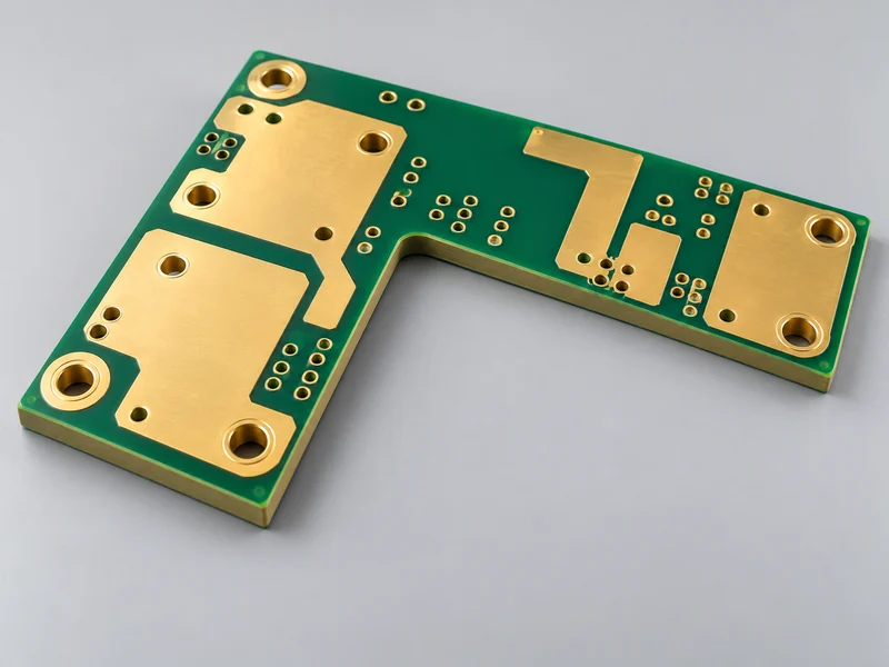
Shape input and output regions around isolation needs, connection points, and the mechanical envelope.
APPLICATIONS
Power stages and distribution boards designed around continuous load, connector interfaces, and temperature rise.
Solar inverters and energy storage converters with coordinated copper paths, dielectric spacing, and cooling.
Motor controls, converters, and automation equipment with defined load cycles and mechanical constraints.
Rectifier and conversion stages requiring a balance of current capacity, routing space, and assembly needs.
PRODUCTION & ENGINEERING
MV Circuit provides PCB fabrication and assembly support for customers across Europe, North America, and Asia. For a heavy copper project, we bring together the fabrication drawing, stack-up, copper requirements, material selection, and assembly data before production begins.
Our team supports CAM and DFM review, incoming material inspection, and traceable production records. A dedicated project contact coordinates technical questions, production updates, and shipment planning, while component sourcing and assembly support help you manage the complete project.
PROCESS PLANNING
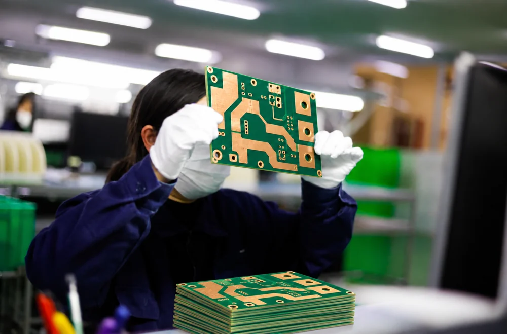
Confirm the copper map, stack-up, drill data, clearances, finish, and acceptance plan.
Apply the agreed imaging, etching, and plating route to create the conductor profile.
Control layer alignment, resin fill, hole preparation, solder mask, and exposed-pad finish.
Complete agreed inspection and electrical tests, then protect the boards for handling and delivery.
TESTING & INSPECTION
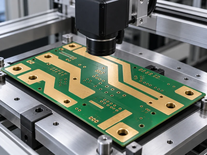
Review conductor geometry, spacing, exposed pads, and mask coverage against the approved artwork and acceptance criteria.
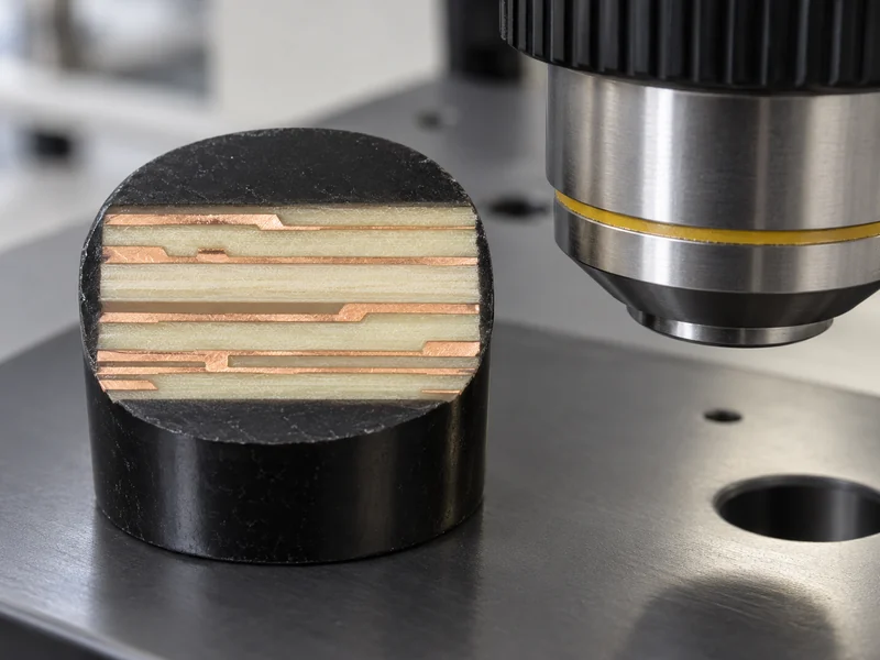
Use agreed sample or coupon inspection to evaluate copper, dielectric construction, and plated-hole quality where specified.
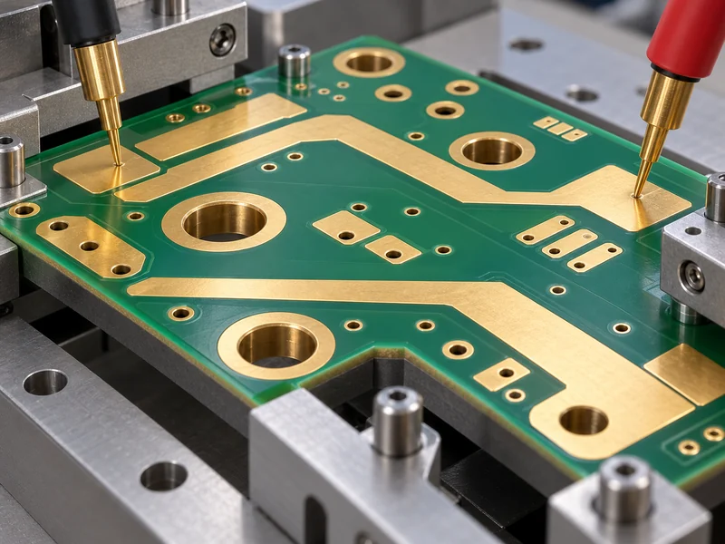
Verify the bare-board net connections and isolation. Loaded current and thermal validation follow a separately defined product test plan.
MANUFACTURING VIDEO
Explore a heavy copper PCB video from our official manufacturing channel. Discuss the copper thickness, layout, and inspection needs for your own build with MV Circuit.
START YOUR PROJECT
Send your fabrication files, drill data, stack-up, finished copper per layer, material grade, board thickness, finish, quantities, and delivery target. Include current and thermal requirements, hole plating, inspection criteria, and assembly data where relevant.
Send Your Heavy Copper PCB Inquiry
Email: info@mv-circuit.com
COMMON QUESTIONS
A heavy copper PCB uses thicker copper conductors than a conventional circuit board to create larger conducting cross-sections. The term is commonly used around 3 oz/ft² and above, although supplier definitions differ. Specify the required finished thickness on each layer rather than relying on the name alone.
Using the conventional nominal conversion of approximately 35 µm per oz/ft², 4 oz is about 140 µm, 6 oz about 210 µm, and 10 oz about 350 µm. These are reference conversions. Your fabrication drawing should define finished thickness, tolerances, and measurement locations.
There is no single current rating for a copper weight. Trace width, finished thickness, layer position, ambient temperature, acceptable temperature rise, copper planes, airflow, and terminal connections all affect the result. Share continuous and peak current requirements so the complete path can be reviewed and validated.
Different copper weights may be specified on different layers of a multilayer build. This can reserve thicker copper for power distribution while retaining practical routing for control signals. The stack-up needs a review of copper balance, resin fill, dielectric spacing, and registration. Different copper thicknesses within one layer require a separate process assessment.
FR-4 and high-Tg FR-4 are common starting points. Select the exact laminate grade against operating temperature, thermal cycling, dielectric needs, moisture exposure, and assembly conditions. Higher Tg alone does not define the allowable continuous operating temperature or qualify the finished board.
Thicker conductors make etching and profile control more demanding. The required line width and gap depend on copper thickness and the fabrication route. Functional voltage clearance and creepage requirements must also be satisfied; a manufacturing minimum is not an electrical safety clearance.
Surface copper weight does not automatically specify the copper thickness on a plated hole wall. Hole diameter, barrel plating, via quantity, layer connections, and thermal distribution must be considered separately. Define hole-wall plating and any coupon or microsection requirements in the fabrication specification.
ENIG, lead-free HASL, OSP, immersion silver or tin, and other specified finishes can be reviewed for the build. The choice depends on soldering, flatness, contact use, storage, and assembly. A surface finish protects exposed copper; it does not replace the required conductor thickness.
MV Circuit can coordinate PCB fabrication, component sourcing, SMT and through-hole assembly, and agreed testing. Send the BOM, placement data, assembly drawings, and thermal or soldering constraints. Large copper areas can affect heat demand during soldering, so the assembly process should be reviewed with the bare board.
Provide Gerber or an agreed fabrication format, drill files, stack-up, finished copper requirements per layer, board thickness, laminate grade, finish, quantities, and delivery target. Add current and thermal requirements, hole-wall plating, inspection criteria, and the BOM for assembly. Price and delivery follow the review of the complete specification.
CUSTOMER FEEDBACK
“The team is highly responsive and always willing to provide expert advice.”Michael S. · USA
“The communication throughout the process is seamless. We highly recommend them for any PCB needs in the future.”Sarah L. · Germany
“Their quick turnaround times and dedication to ensuring we meet our deadlines make them an invaluable partner for us.”John D. · Italy
Excerpts from existing feedback about MV Circuit’s general PCB services. Read the original customer feedback.