
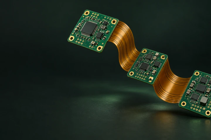
Integrated Rigid & Flexible Circuits
Rigid-Flex PCB Manufacturing & Assembly
Connect rigid board sections through integrated flexible circuits. Bring your electrical layout, folded geometry, and assembly requirements together with MV Circuit.
Get Your Rigid-Flex PCB QuoteOne Circuit, Multiple Planes
Rigid-flex combines component-bearing rigid regions and flexible interconnections in one PCB structure. Plan the board in its final folded shape, with the electrical and mechanical requirements reviewed together.
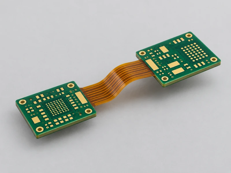
Rigid-Flex PCB Advantages
Build Around Your Assembly
Integrate Board Connections
Replace selected separate cables and board-to-board connectors with integrated circuit connections. Suitability depends on current, signal needs, and serviceability.
Fit Three-Dimensional Layouts
Position rigid board sections on different planes inside the enclosure, using a defined flex length and bend geometry.
Coordinate Fabrication & Assembly
Review component mounting, folded clearances, carriers, and the assembly sequence before releasing the design.
Design the Transition Carefully
Define the rigid-to-flex boundaries, coverlay, routing, and mechanical constraints as part of a coordinated stack-up.
Material Construction
Match Rigid Laminates, Flex Materials & Bonding
Select the complete construction for each region. Material names alone do not establish compatibility or bend performance.
| Region | Listed Material Options | Engineering Review |
|---|---|---|
| Flexible circuitry | Shengyi SF305; Panasonic R-F775(ER); DuPont Pyralux AP | PI and copper thickness, adhesive construction, movement |
| Rigid regions | ITEQ IT-180A; Shengyi S1141 / S1000-2; additional CCL families | Stack-up, thermal requirements, electrical performance |
| Bonding & protection | No-flow prepreg, coverlay, adhesives, PI reinforcement | Rigid-flex boundaries, openings, lamination compatibility |
View all listed laminate, coverlay, adhesive, and reinforcement options
| Parameter | Standard | Advanced | Conditions |
|---|---|---|---|
| Adhesive FCCL | Shengyi SF305: PI 0.5 / 1 / 2 mil; Cu 0.33 / 0.5 / 1 oz | — | — |
| Adhesiveless FCCL | Panasonic R-F775(ER): PI 1 / 2 mil; Cu 0.33 / 0.5 / 1 oz | PI 3 mil; Cu 2 oz | — |
| Adhesiveless FCCL | DuPont Pyralux AP: PI 1 / 2 / 3 mil; Cu 0.5 / 1 oz | PI 4 mil; Cu 2 oz | — |
| Coverlay | Shengyi SF305C 0515 / 0525 / 1025 / 2030; Taiflex FHK 1025 / 1035 | — | — |
| Adhesive | Taiflex BT 10 / 25 / 40 μm; Shengyi SF302B 35 / 40 μm | — | — |
| PI stiffener | Taiflex MHK 3 / 5 / 7 / 9 mil | — | — |
| 3M materials | 9077 / 6677 / 9458 | — | — |
| No-flow prepreg | VT-47N (Tg 170°C); EM-285B (Tg 150°C) | Ventec VT-901 | — |
| Rigid CCL | ITEQ IT-180A; Shengyi S1141 / S1000-2 | — | — |
| Other CCL | Arlon 85N; Rogers RO4000 series; Nelco N4000-13 series; Ventec VT-901 | Ventec VT-901 | Exact material combination subject to review |
Product Configurations
Rigid-Flex Structures for Your Layout
Two Rigid Regions
A direct rigid-flex connection for an assembly with two board positions.
- Define the unfolded flex length and final board spacing.
- Provide the folded orientation and component height limits.
- Coordinate routing through the transition regions.
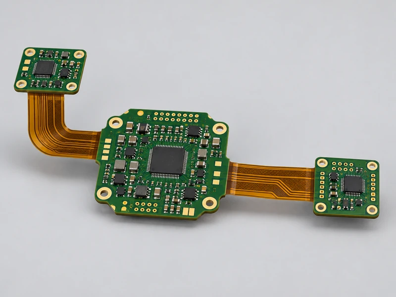
Branched Rigid-Flex
Multiple rigid islands connected through a coordinated flex layout.
- Identify every rigid region and flex branch.
- Review routing, assembly access, and folded clearances.
- Specify the layer continuity through each flex section.
Folded Assembly
Rigid regions arranged in three dimensions for the final enclosure.
- State whether the bend is static or repeatedly moving.
- Include bend radius, direction, and any cycle requirements.
- Confirm tooling, handling, and the inspection plan.
Manufacturing Capabilities
Rigid-Flex PCB Standard & Advanced Capabilities
Process ranges from MV Circuit’s 2024 rigid-flex capability sheet. Advanced items require special checks; final combinations are confirmed for your design.
| Parameter | Standard | Advanced | Conditions |
|---|---|---|---|
| Total layers | 2–12 (up to 10 flex layers) | 13–20 (up to 18 flex layers) | Confirm actual region stack-ups |
| Board thickness | 0.3–3.0 mm | 0.3–4.0 mm | — |
| Thickness tolerance, >1.0 mm | ±10% | — | — |
| Thickness tolerance, ≤1.0 mm | ±0.1 mm | — | — |
| Minimum board size | 10 × 15 mm | — | — |
| Maximum board size | 406.4 × 558.8 mm | 406.4 × 736.6 mm | — |
| Single-ended impedance | ±5 Ω at ≤50 Ω; ±10% at >50 Ω | ±3 Ω at ≤50 Ω; ±8% at >50 Ω | — |
| Differential impedance | ±5 Ω at ≤50 Ω; ±10% at >50 Ω | ±4 Ω at ≤50 Ω; ±8% at >50 Ω | — |
| HDI | — | 1+n+1; buried via ≤0.4 mm | Special checks required |
| Bow and twist | 0.75% symmetrical; 2% unsymmetrical | 1.5% unsymmetrical | — |
Full board, interconnection, drilling, and outline specifications
| Parameter | Standard | Advanced | Conditions |
|---|---|---|---|
| Total layers | 2–12 (up to 10 flex layers) | 13–20 (up to 18 flex layers) | Confirm actual region stack-ups |
| Board thickness | 0.3–3.0 mm | 0.3–4.0 mm | — |
| Thickness tolerance, >1.0 mm | ±10% | — | — |
| Thickness tolerance, ≤1.0 mm | ±0.1 mm | — | — |
| Minimum board size | 10 × 15 mm | — | — |
| Maximum board size | 406.4 × 558.8 mm | 406.4 × 736.6 mm | — |
| Single-ended impedance | ±5 Ω at ≤50 Ω; ±10% at >50 Ω | ±3 Ω at ≤50 Ω; ±8% at >50 Ω | — |
| Differential impedance | ±5 Ω at ≤50 Ω; ±10% at >50 Ω | ±4 Ω at ≤50 Ω; ±8% at >50 Ω | — |
| HDI | — | 1+n+1; buried via ≤0.4 mm | Special checks required |
| Bow and twist | 0.75% symmetrical; 2% unsymmetrical | 1.5% unsymmetrical | — |
| Ecoobond width | 1.5 ±0.5 mm | 1.2 ±0.5 mm | Flex window width ≥5 mm |
| Inner blind-via annular ring | 4 mil | 3 mil | — |
| Maximum inner copper | 2 oz | 3 oz | — |
| Minimum BGA pad | 12 mil; 8 mil for electrolytic soft-gold boards | 10 mil; 7 mil for electrolytic soft-gold boards | — |
| Maximum finished outer copper | 3 oz | 5 oz | — |
| Blind via | — | 4–6 mil; 6 mil preferred | — |
| Maximum buried via | 0.4 mm | — | — |
| Mechanical drill aspect ratio | 10:1 | 12:1 | — |
| Laser drill aspect ratio | — | 0.8:1 | — |
| Via-to-conductor clearance, ≤6 layers | 6 mil | 5 mil | — |
| Via-to-conductor clearance, 7–11 layers | 9 mil | 7 mil | — |
| Via-to-conductor clearance, ≥12 layers | 12 mil | 9 mil | — |
| Blind-via-to-conductor clearance | — | 6 mil | 1-step HDI |
| Non-plated hole tolerance | ±2 mil | — | Limit options +0/−2 mil or +2/−0 mil |
| Routed outline tolerance | ±6 mil | ±4 mil | Standard excludes complicated outlines and cutouts |
Trace width / spacing by copper thickness and surface-flex construction
Values are width / spacing in mil. Parenthesized values are listed as partial capability and require confirmation.
| Parameter | Standard | Advanced | Conditions |
|---|---|---|---|
| Inner, 12/18 μm Cu | 3.5 / 3.5 (3.2 / 3.2) | 3.0 / 3.0 (2.8 / 2.5) | mil |
| Inner, 35 μm Cu | 4.0 / 4.0 (3.6 / 3.7) | 3.5 / 3.5 (3 / 3.1) | mil |
| Inner, 70 μm Cu | 6 / 6.5 (5.5 / 6) | 5 / 6 (4.5 / 5.5) | mil |
| Outer, 18 μm Cu | 3.5 / 3.8 (3.2 / 3.5) | 3.2 / 3.6 (3.0 / 3.3) | mil |
| Outer, 35 μm Cu | 4.0 / 4.3 (3.5 / 3.8) | 3.5 / 3.8 (3.3 / 3.6) | mil |
| Outer, 70 μm Cu | 6.5 / 6 (6 / 5.5) | 6.0 / 5.5 (5.5 / 5) | mil |
| Outer, 105 μm Cu | 10 / 13 (9.5 / 12.5) | 9.5 / 12.5 (9 / 12) | mil |
| Surface-flex outer, 18 μm Cu | 5 / 5 (4.5 / 4.5) | 4.5 / 4.5 (4 / 4) | mil |
| Surface-flex outer, 35 μm Cu | 5.5 / 6 (5 / 5.5) | 5 / 5.5 (4.5 / 5) | mil |
| Surface-flex outer, 70 μm Cu | 7.0 / 8.0 (6.5 / 7.5) | 6.5 / 7.5 (6 / 7.0) | mil |
Mask, silkscreen, surface finishes, and plating thicknesses
| Parameter | Standard | Advanced | Conditions |
|---|---|---|---|
| Mask colors | Green, blue, red, matte green | White, black, matte black | — |
| Minimum mask dam, Cu ≤1 oz | 4 mil green/red/blue; 5 mil black/white | — | Color qualification still applies |
| Minimum mask dam, Cu 2–4 oz | 8 mil | 6 mil | — |
| Minimum mask clearance | 2.5 mil (2.0 mil) | 2.0 mil (1.5 mil) | Parentheses: partial capability |
| Plugged-hole diameter | — | 0.2–0.5 mm | — |
| Non-conductive resin plug aspect ratio | — | 10:1 | — |
| Silkscreen colors | White / yellow / black | — | — |
| Finishes | HASL / lead-free HASL, ENIG, ENEPIG, electrolytic nickel gold, soft gold, hard gold, immersion silver, immersion tin, OSP | — | — |
| Mixed finishes | ENIG + OSP; ENIG + gold fingers; electrolytic gold + gold fingers | — | — |
| ENIG thickness | Au 0.05–0.10 μm; Ni 3–8 μm | — | — |
| ENEPIG thickness | Au 0.05–0.10 μm; Pd 0.05–0.15 μm; Ni 3–8 μm | — | — |
| Hard gold thickness, lead-free | 0.1–1.5 μm | — | — |
| Hard gold thickness, including lead | 0.1–4.0 μm | — | As labeled in capability sheet; confirm specification |
| Electrolytic nickel / gold | Ni ≥3 μm; Au 0.05–0.10 μm | — | — |
| Immersion silver | 0.2–0.4 μm | — | — |
| OSP | 0.1–0.3 μm | — | — |
A dash means no separate value is listed in the source sheet. Individual minimums and maximums are not assumed to be simultaneously achievable. Bend radius and repeated-flex performance require a construction-specific review.
Product Gallery
Explore Rigid-Flex PCB Configurations
Discuss the rigid regions, flexible connections, and final assembly shape for your project.
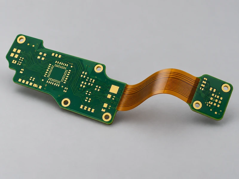
Two Rigid Regions
A direct rigid-flex connection for an assembly with two board positions.
Discuss Your Project →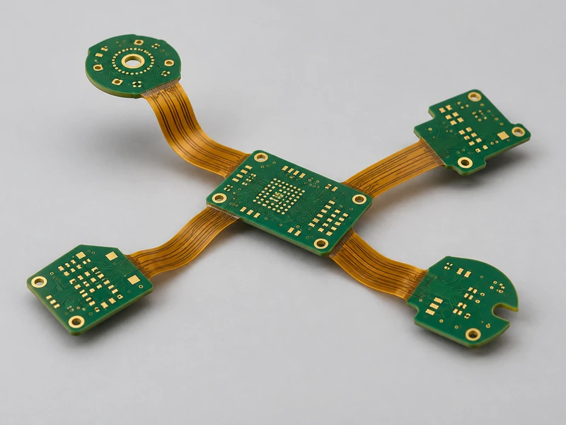
Branched Rigid-Flex
Multiple rigid islands connected through a coordinated flex layout.
Discuss Your Project →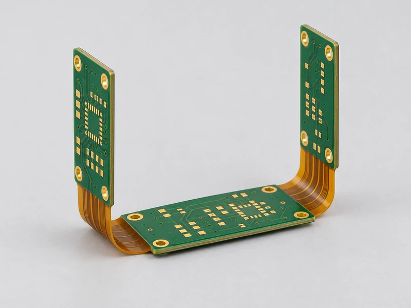
Folded Assembly
Rigid regions arranged in three dimensions for the final enclosure.
Discuss Your Project →About MV Circuit
MV Circuit: Your Rigid-Flex Manufacturing Partner
Dedicated Support for Rigid-Flex Projects
At MV Circuit, your rigid-flex project is managed as a complete circuit and assembly. Our team reviews the fabrication files with your rigid and flexible stack-ups, transition boundaries, and folded drawings, helping resolve engineering questions before manufacturing begins.
A dedicated project manager coordinates engineering, production, and delivery, with weekly work-in-process updates and lot-level traceability. We support DFM, DFA, and DFT reviews alongside component sourcing and SMT assembly, so fabrication and assembly requirements can be addressed together. Electrical testing and AOI inspection form part of our quality process, with additional acceptance requirements agreed for your application.
Watch Rigid-Flex PCB Manufacturing
Explore rigid-flex manufacturing in this video from the PCBMay official channel. Share your fabrication data, region stack-up, and folded assembly drawing for a project review.
- Fabrication files: RS-274-D / RS-274-X Gerber.
- Drill data: Excellon format.
- Mechanical details: rigid-flex boundaries, bend directions, and final folded geometry.
Quality & Validation
Review the Board as a Complete Assembly
01
Electrical Verification
Define continuity, isolation, and any impedance or application-specific verification in the agreed inspection plan.
02
Mechanical & Folded Fit
Check rigid outlines, transition regions, flex lengths, hole positions, and the final folded assembly against your drawing.
03
Assembly & Handling
Review support tooling, component placement, soldering sequence, and any bend or environmental validation required by the application.
Start Your Project
Request Your Rigid-Flex PCB Quote
Send Gerber and Excellon files, the full rigid and flexible stack-up, unfolded and folded drawings, quantity, and delivery requirements. Include the BOM and placement files for assembly.
Send Your Rigid-Flex PCB InquiryEmail: info@mv-circuit.com
Common Questions
Rigid-Flex PCB FAQ
How is rigid-flex different from a flex cable connecting two boards?
Rigid-flex integrates rigid and flexible regions into one PCB structure. A separate flex cable uses connections between individually manufactured parts.
Why do you need a folded assembly drawing?
It shows the final arrangement, bend directions, and clearances so mechanical requirements can be reviewed alongside fabrication data.
Can rigid-flex PCBs bend repeatedly?
Repeated bending requires an application-specific flex construction and validation. Explain the movement, bend radius, and expected cycles before manufacturing.
How do you define the rigid and flexible layer stack-ups?
Provide one coordinated stack-up showing which layers continue through each region. Include material, thickness, and copper information for both rigid and flexible portions.
What is a rigid-to-flex transition area?
It is the boundary between the rigid board and the flexible section. Routing, coverlay edges, clearances, and mechanical stress at this boundary need coordinated review.
Can rigid-flex replace board-to-board connectors?
It can replace selected connectors and cables when the electrical and mechanical design allows. Review assembly access, serviceability, current requirements, and movement before choosing the structure.
Can components be placed close to a bend?
Avoid treating the bend as a normal component mounting area. Define bend zones and component clearances in the mechanical drawing and have the proposed layout reviewed before release.
What assembly support may be needed?
Support tooling or carriers may be required to hold flexible areas during printing, placement, soldering, and inspection. Share the assembly sequence and component layout for review.
How should a rigid-flex prototype be validated?
Define electrical checks, dimensional inspection, folded fit, assembly conditions, and any required bend or environmental testing according to the intended application.
What drives rigid-flex price and delivery time?
The combined stack-up, number of rigid regions, flex construction, outline, panel utilization, assembly tooling, quantity, and testing requirements affect both price and schedule.
Customer Feedback
What Our Customers Say
“The team at MV Circuit consistently delivers high-quality printed circuit boards and exceptional customer service. Their quick turnaround times and dedication to ensuring we meet our deadlines make them an invaluable partner for us.”
John D. · Italy
Existing feedback about MV Circuit’s overall PCB service. View the original feedback.