

HIGH DENSITY INTERCONNECT SOLUTIONS
HDI PCB Manufacturing & Assembly
Make room for fine-pitch components and complex routing. MV Circuit brings your HDI stack-up, microvia design, and assembly requirements into one coordinated manufacturing review.
Get Your HDI PCB QuoteCOMPACT DESIGN. DENSE CONNECTIONS.
More Connections in Less Board Space
HDI technology combines fine routing with microvia interconnections to support compact electronic designs. Plan the component escape routing and layer structure together to balance board area, manufacturing complexity, and reliability.
HDI PCB ADVANTAGES
Design for Density from the Start
Route Fine-Pitch Components
Create routing paths around dense pad arrays by coordinating trace geometry, microvia positions, and layer assignments.
Use Board Area Efficiently
Local layer-to-layer connections can free routing space compared with through-vias that occupy every layer. The benefit depends on the actual layout.
Plan the Signal Path
Select layer transitions and reference planes with your impedance and signal requirements in mind. HDI construction alone does not guarantee signal performance.
Coordinate Fabrication & Assembly
Review via-in-pad, copper filling, solderable pad surfaces, and fine-pitch component requirements before releasing the manufacturing data.
MATERIAL SELECTION
Build the Stack-Up Around Your Application
Choose the laminate system together with the build-up dielectric, copper construction, and assembly temperature profile.
FR-4 & High-Tg Systems
Review thermal requirements and sequential lamination compatibility alongside the proposed layer structure.
High-Frequency Materials
Match dielectric properties and copper construction to the frequency range and loss targets of your design.
Hybrid Constructions
Coordinate dissimilar material systems, thicknesses, and processing requirements before committing to a hybrid stack-up.
HDI BUILD-UP OPTIONS
Choose Your HDI Interconnection Structure
The build-up notation describes the layer construction. Product views below illustrate possible board layouts; the final via arrangement is defined by your stack-up and drill data.
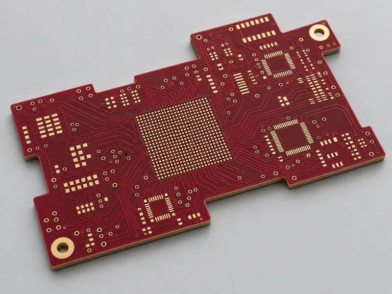
1+N+1 HDI
One build-up layer on each side of the core, selected when a single microvia level meets the escape-routing needs.
- Define the core and outer dielectric layers.
- Identify microvia start and stop layers.
- Review BGA escape routing before layout release.
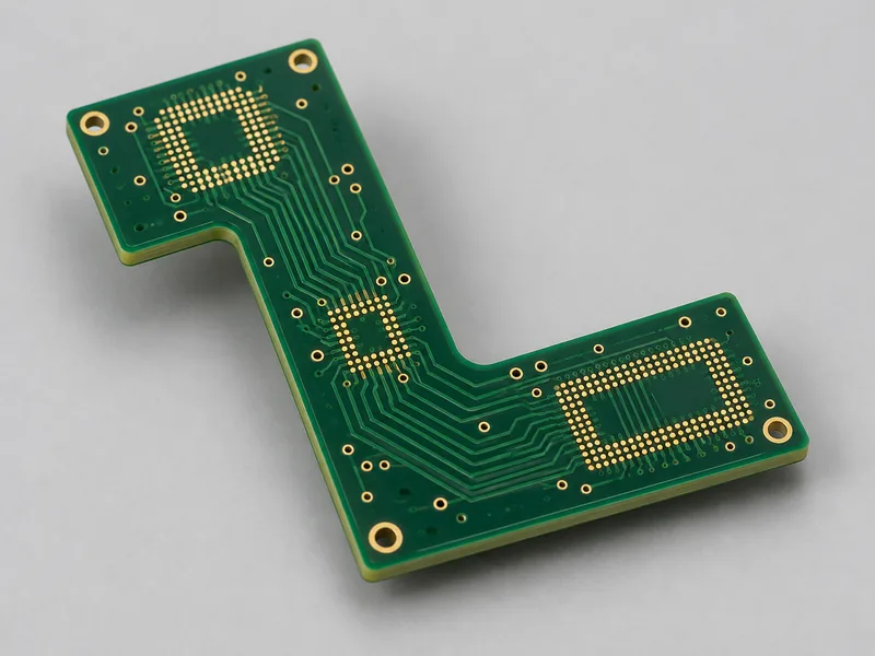
2+N+2 HDI
Two build-up layers per side create additional interconnection options for a more demanding routing plan.
- Specify stacked or staggered connections.
- Review copper filling and target-pad geometry.
- Coordinate sequential lamination with material selection.
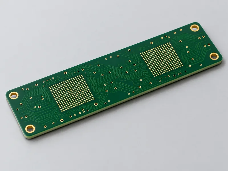
3+N+3 HDI
Three build-up layers per side for designs requiring a more complex layer-to-layer connection strategy.
- Provide the complete via connection matrix.
- Review the full manufacturing sequence.
- Agree verification for the selected construction.
MANUFACTURING CAPABILITIES
HDI PCB Standard & Advanced Capabilities
| Feature | Standard Capabilities | Advanced Capabilities |
|---|---|---|
| Layer Count | 1–20 Layers | 22–40 Layers |
| Blind & Buried Via Type (Mechanical) | Mechanical blind & buried vias with less than 3 times laminating | Mechanical blind & buried vias with less than 2 times laminating |
| HDI Structure | 1+N+1, 2+N+2, 3+N+3 (Buried vias ≤0.3mm) | 1+n+1, 1+1+n+1+1, 2+n+2, 3+n+3 (n buried vias ≤0.3mm). Laser blind via can be filling plating |
| Laser Via Drill Size | Min 4mil / Max 6mil | Min 4mil / Max 6mil |
| Technology | Laser Blind Vias (Copper Filling), Standard Pad Density | High Pad Density, Fine Microvias, Surface Pads |
| Min. Trace/Gap | 0.075mm / 0.075mm | 0.05mm / 0.05mm |
| Copper Weight | 0.5 oz – 4 oz (18μm – 70μm) | 0.3 oz up to 100 oz |
| Board Thickness | 0.2mm – 3.2mm | 3.4mm – 10.0mm |
| Max Board Size | 500mm × 600mm | 1100mm × 500mm |
| Base Materials | KB, Shengyi, Shengyi SF305, FR408, FR408HR, IS410, FR406, GETEK, 370HR, IT180A, Rogers4350, Rogers400, PTFE Laminates (Rogers, Taconic, Arlon, Nelco), Hybrid With FR-4 | Same as Standard |
| Surface Finish | Immersion Tin, Immersion Silver, Electrolytic Gold, Gold Fingers, OSP, ENIG | Same as Standard |
PRODUCT GALLERY
Explore HDI PCB Layouts
Discuss your board outline, component density, and interconnection requirements with our team.
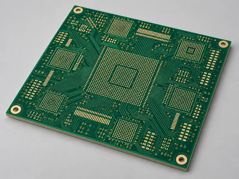
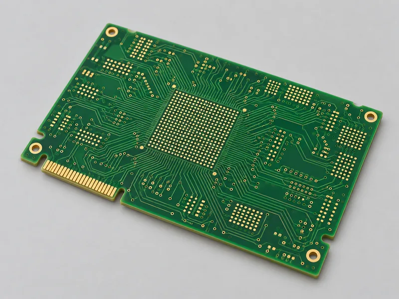
Dense BGA Routing
A compact layout with a central pad array and tightly coordinated escape routing.
Discuss Your Project →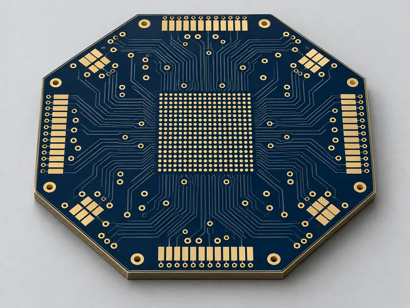
Space-Constrained Layouts
A shaped board outline that accommodates the mechanical envelope of your product.
Discuss Your Project →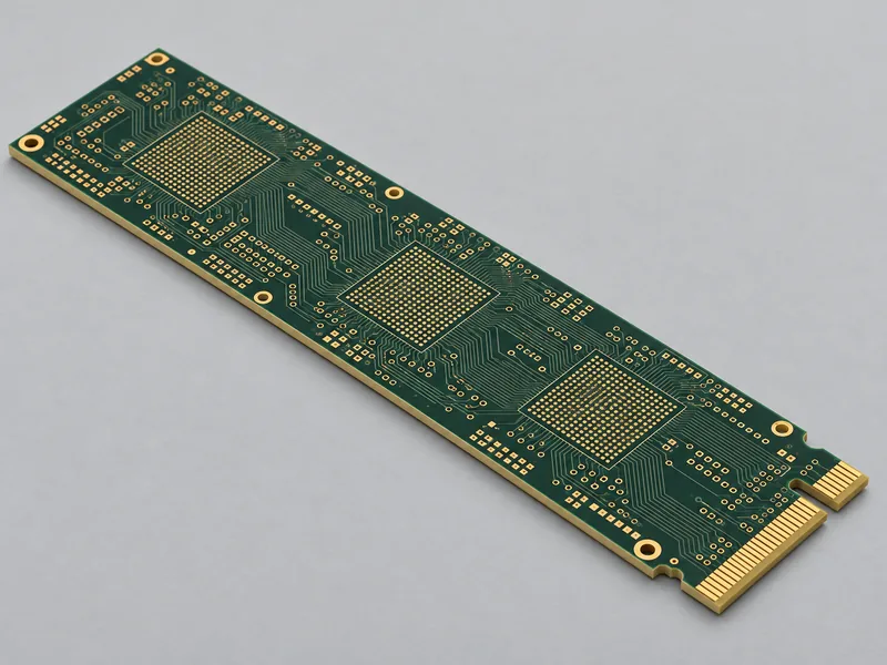
Module Interconnections
An elongated layout with multiple dense component regions and connected routing channels.
Discuss Your Project →ABOUT MV CIRCUIT
Your HDI Project, Supported from Data to Delivery
Engineering Detail. Coordinated Production.
MV Circuit supports HDI fabrication and assembly as one connected project. Our team reviews your artwork, layer stack-up, drill definitions, and assembly needs before manufacturing, helping identify engineering questions while changes are still easier to make.
A dedicated project manager coordinates the handover from CAM review to production. Component sourcing, SMT assembly, inspection, and testing can be included in the project scope. Weekly work-in-process updates and traceable production records keep you informed as your order progresses.
Watch PCB Laser Drilling
Laser drilling is one of the processes used to form HDI microvias. Watch this manufacturing video from the PCBMay official channel.
Share your intended layer pairs, dielectric construction, and via filling requirements so the manufacturing sequence can be reviewed with your complete design.
Watch on YouTubeQUALITY & VALIDATION
Review the Interconnections, Not Just the Outline
Artwork & Layer Review
Check pad geometry, routing, target layers, and drill definitions against the agreed manufacturing construction.
Inspection & Electrical Test
Use AOI and electrical testing within the production quality plan. Define additional microsection or impedance requirements for your project.
Application Qualification
Agree any thermal, assembly, or reliability validation needed for the actual via structure and operating conditions.
START YOUR PROJECT
Request Your HDI PCB Quote
Send fabrication artwork, drill data, the complete stack-up, via definitions, quantity, and delivery requirements. Include impedance targets, filling specifications, and the BOM and placement data for assembly.
Send Your HDI PCB InquiryEmail: info@mv-circuit.com
COMMON QUESTIONS
HDI PCB FAQ
What is an HDI PCB?
A high-density interconnect PCB uses features such as laser microvias and fine routing to connect dense component layouts. Its construction is selected around the component pitch, required routing channels, and electrical requirements.
What do 1+N+1 and 2+N+2 mean?
The outer numbers describe build-up layers on each side of the central N-layer core. A 1+N+1 construction has one build-up layer per side; 2+N+2 has two. The fabrication drawing should also define the connections between each layer pair.
Should I choose stacked or staggered microvias?
Staggered microvias are offset between build-up levels; stacked microvias align vertically. Selection depends on available routing space, pad design, filling and capping, and the reliability requirements of the finished product. Ask for a stack-up review before fixing the via arrangement.
Does an HDI PCB always need via-in-pad?
No. Via-in-pad is useful when component escape routing or space makes it necessary. Where a via lies in a solderable pad, specify the filling, capping, and surface planarity requirements so assembly needs can be reviewed.
How do I select materials for an HDI stack-up?
Consider dielectric thickness, copper profile, signal loss, thermal behavior, and compatibility with sequential lamination. Share the operating environment and electrical targets; a material name on its own does not define the complete construction.
Can laser microvias and mechanical vias be used together?
Yes. An HDI design may combine laser blind microvias with mechanically drilled through or buried vias. The drill and layer-pair data must clearly identify each connection and the proposed manufacturing sequence.
What files are required for an HDI PCB quotation?
Provide fabrication artwork, drill data, a complete stack-up, via definitions, board outline, quantity, and delivery requirements. Add impedance targets and acceptance criteria. Include the BOM and placement files when requesting assembly.
How are microvia quality and reliability evaluated?
Agree the inspection and qualification plan for the actual construction. Electrical testing checks connectivity, while microsections and appropriate thermal or reliability testing can examine interconnection quality. A continuity result alone does not establish lifetime reliability.
Can MV Circuit supply assembled HDI boards?
We support fabrication together with component sourcing, SMT assembly, and testing. Share the BOM, placement data, fine-pitch package details, and any inspection or functional test requirements with the fabrication package.
What affects HDI PCB cost and lead time?
Build-up complexity, lamination cycles, via filling, materials, layer count, panel utilization, inspection, and order quantity all influence the quotation. The delivery schedule is confirmed after engineering review and material availability checks.
CUSTOMER FEEDBACK
What Our Customers Say
“Their attention to detail and commitment to delivering high-quality PCBs on time has helped streamline our production process. The team is highly responsive and always willing to provide expert advice.”
Michael S. · USA
Existing feedback about MV Circuit’s overall PCB service. View the original feedback.