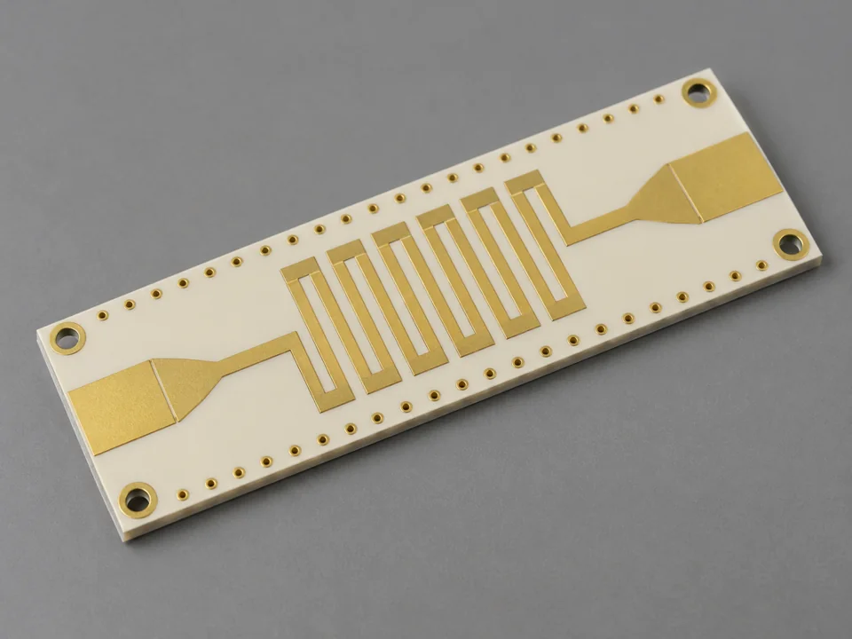
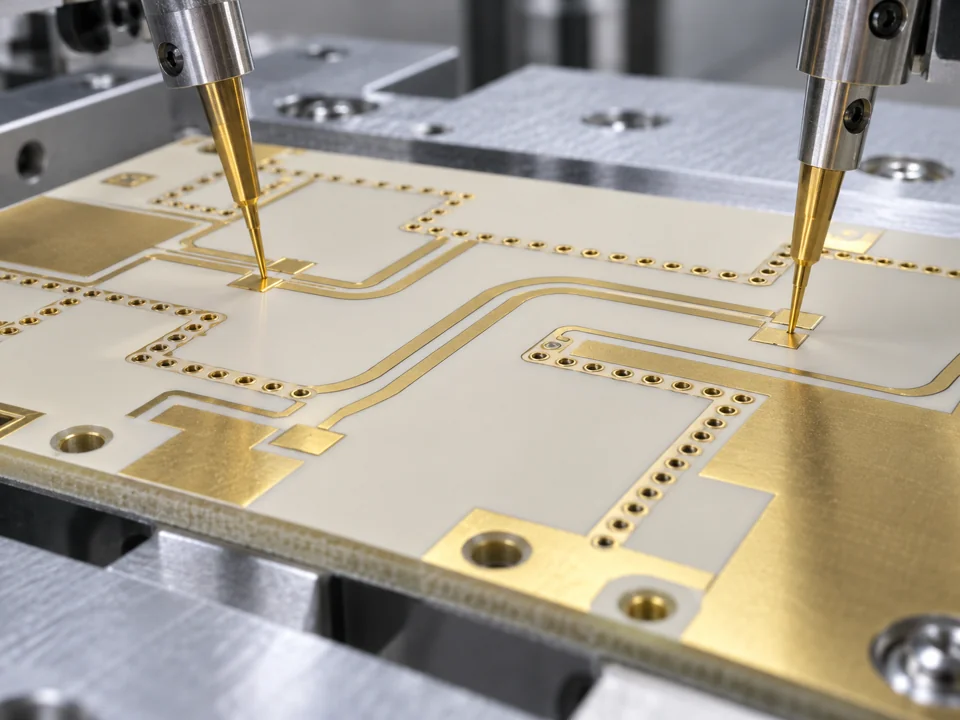
RF Filters & Couplers
Controlled conductor shapes, gaps, and ground structures for frequency-selective signal paths.
Discuss Your Filter Board →
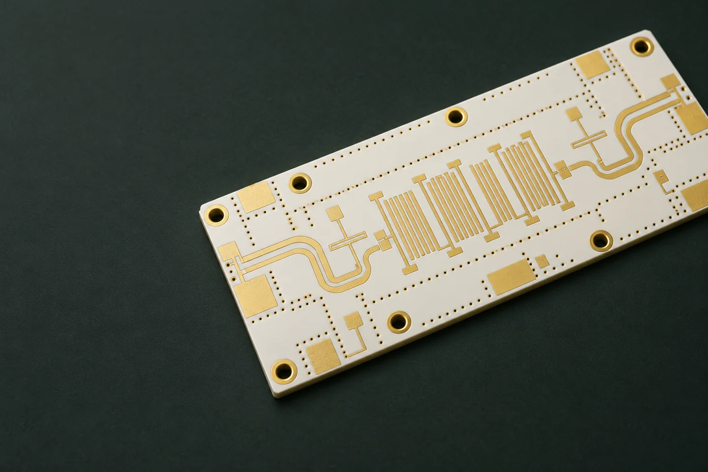
RF & MICROWAVE CIRCUIT BOARDS
Custom high-frequency PCBs for RF signal paths, antennas, and microwave electronics. Coordinate the Rogers laminate, copper structure, stack-up, and inspection plan with MV Circuit before production.
Get Your Rogers PCB QuoteHIGH-FREQUENCY MATERIALS
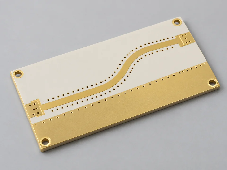
A Rogers PCB uses a specified laminate from Rogers Corporation for part or all of its dielectric construction. The material family, thickness, copper foil, and fabrication geometry work together to determine electrical behavior.
MV Circuit supports Rogers PCB inquiries for prototypes and production, including RF layouts, antenna boards, and hybrid multilayer designs. We review the complete build rather than treating every Rogers grade as an interchangeable replacement for FR-4.
Share your operating frequency, stack-up, impedance targets, mechanical drawing, and acceptance requirements. We will coordinate the material and manufacturing review before confirming the quotation.
Discuss Your RF PCBDESIGN PRIORITIES
For a long or sensitive RF path, the dielectric loss budget can influence laminate selection. Compare material data at the relevant test conditions alongside conductor loss, copper profile, connectors, and routing length.
Process Dk and design Dk are different data sets. Use the value and model appropriate to the transmission-line geometry and simulation method, then validate the finished design where required.
Dielectric thickness, thermal expansion, dimensional behavior, plated-hole construction, and the assembly environment all belong in the material review. No single property establishes the best laminate for every product.
A hybrid construction can reserve RF laminate for critical layers while using suitable FR-4 elsewhere. Bonding compatibility, symmetry, copper distribution, and inspection access must be assessed together.
MATERIAL SELECTION
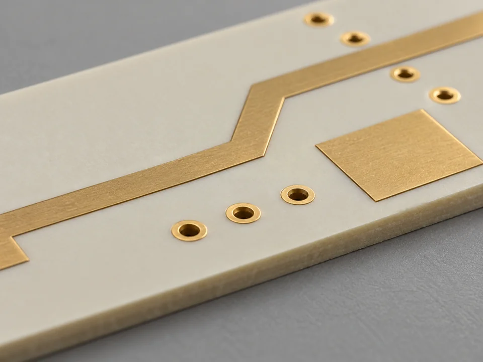
The RO4000 family and PTFE-based products have different processing and electrical characteristics. Specify the exact grade and revision of the data sheet, dielectric thickness, copper cladding, and any approved alternatives.
Material availability and the proposed build are confirmed during quotation. A supplier’s laminate property is not a finished-board performance guarantee.
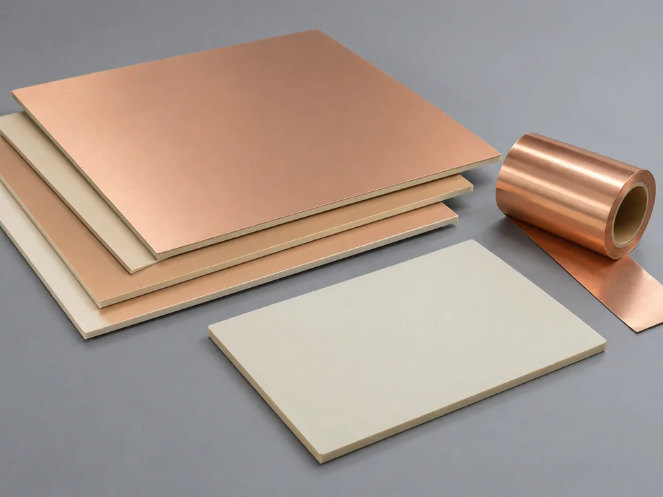
| Laminate | Process Dk | Design Dk | Typical Df at 10 GHz | Selection focus |
|---|---|---|---|---|
| RO4003C™ | 3.38 ± 0.05 | 3.55 | 0.0027 | RF circuits and multilayer builds using a hydrocarbon/ceramic laminate system. |
| RO4350B™ | 3.48 ± 0.05 | 3.66 | 0.0037 | RF construction where the grade’s flame-retardant properties are relevant. |
| RO4835™ | 3.48 ± 0.05 | 3.66 | 0.0037 | Low-loss thermoset construction with improved oxidation resistance. |
| RT/duroid® 5870 | 2.33 ± 0.02 | 2.33 | 0.0012 | Glass-microfiber-reinforced PTFE for low-Dk RF structures. |
| RT/duroid® 5880 | 2.20 ± 0.02 | 2.20 | 0.0009 | Low-Dk, low-loss PTFE-based microwave construction. |
Values above are supplier-published reference data, not fabrication acceptance limits. Process Dk is listed at approximately 10 GHz; RO4000 design values and RT/duroid design values use different characterization methods and conditions. Refer to the linked data sheets for the applicable thickness, direction, frequency, and test method.
RO3000 series, TMM materials, specialized thermal-management grades, and compatible bonding systems can be reviewed when the design requires them. Send the exact part designation and construction; different grades are not automatic substitutes.
CONSTRUCTION OPTIONS
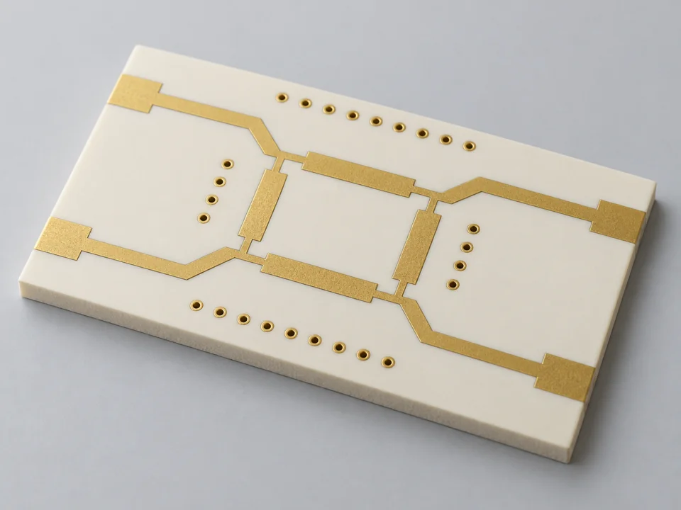
Consider RO4003C, RO4350B, or RO4835 when the electrical design and the grade’s thermoset processing characteristics fit the project.
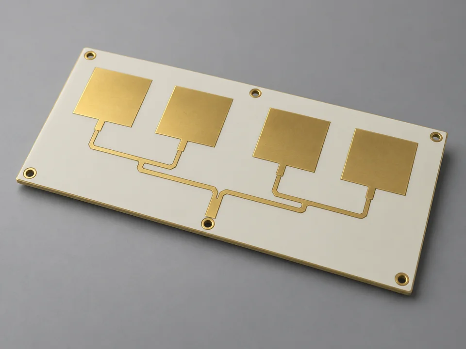
RT/duroid and other PTFE families need material-specific drilling, hole-wall preparation, handling, and bonding decisions.
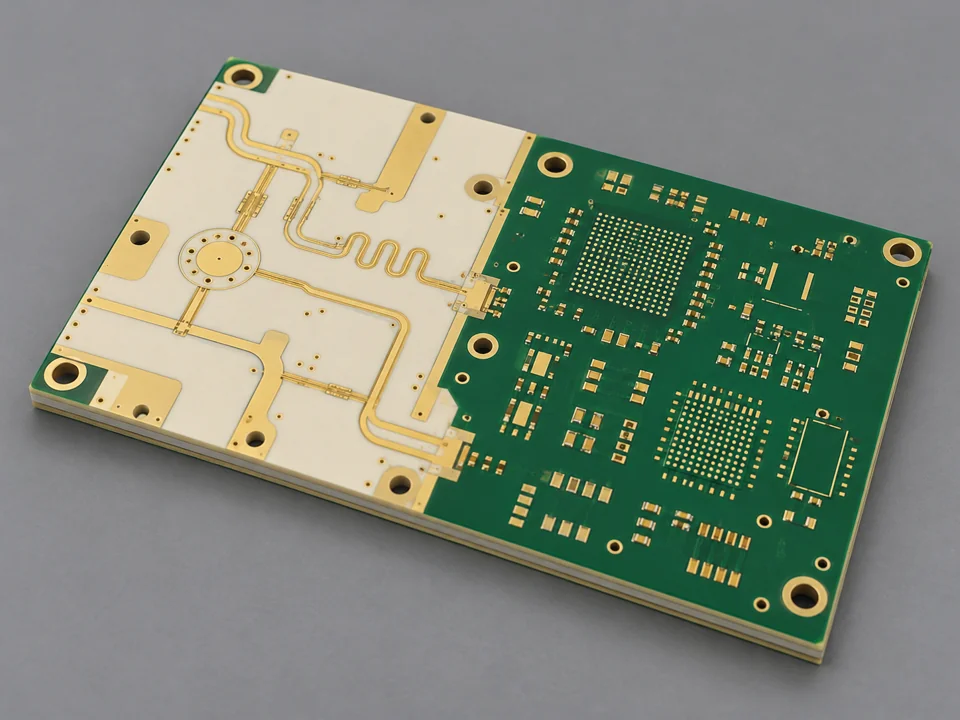
Combine the required RF dielectric layers with suitable FR-4 regions or layers where the complete bonding system and thermal behavior permit.
Product images illustrate possible circuit layouts. A photograph alone cannot identify a laminate grade or verify a finished RF specification.
FABRICATION REVIEW
The available geometry and process route depend on the chosen laminate, copper, thickness, layer structure, and inspection plan. We confirm the combined requirements during engineering review.
| Feature | Project review |
|---|---|
| Materials | Exact Rogers grade, data sheet, dielectric thickness, copper foil, bonding system, and approved alternatives. |
| Layer structure | Double-sided, multilayer, or Rogers/FR-4 hybrid construction subject to the approved stack-up. |
| RF geometry | Trace width and gap, conductor thickness, reference planes, via fences, launches, and copper-to-edge details. |
| Interconnections | Plated and non-plated holes, slots, via pairs, filling requirements, aspect ratio, and material-specific hole preparation. |
| Controlled impedance | Target, tolerance, layer, geometry, reference plane, and coupon or measurement requirements agreed before production. |
| Surface treatment | ENIG, immersion silver, OSP, selective gold, or another agreed finish selected for the soldering, contact, and RF requirements. |
| Inspection | AOI, electrical test, dimensional checks, and agreed microsection, impedance, or additional qualification requirements. |
| Assembly | Component sourcing, SMT, inspection, and specified testing with the BOM, placement data, and assembly drawings. |
Bare-board connectivity testing does not measure a finished system’s insertion loss, return loss, antenna efficiency, or radiated performance. If RF measurements are required, define the frequency range, fixture, calibration, coupon geometry, method, and acceptance limits before quotation.
RO4000 thermoset laminates and PTFE-based systems do not share one universal process recipe. Drilling, metallization, bonding, dimensional compensation, and handling are selected for the actual material combination. Generic FR-4 settings should not be assumed to apply to every Rogers construction.
PRODUCT GALLERY
Discuss these common RF layout approaches with our team. Final dimensions, materials, finishes, and electrical validation follow your approved files.
Controlled conductor shapes, gaps, and ground structures for frequency-selective signal paths.
Discuss Your Filter Board →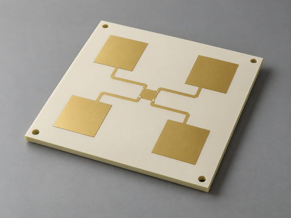
Plan dielectric thickness, patch dimensions, feed geometry, and mechanical integration together.
Discuss Your Antenna PCB →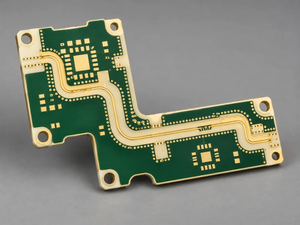
Coordinate dense footprints, grounding, signal launches, and the enclosure interface.
Discuss Your RF Module →APPLICATIONS
Antenna feeds, RF front ends, and communication links with defined loss and impedance requirements.
Transmission-line and antenna structures where geometry and dielectric selection affect tuning.
RF subsystems with application-specific material, thermal, and qualification requirements.
Signal routing and reference structures for instruments, fixtures, and RF development platforms.
Suitability depends on the complete design and qualification plan; choosing a laminate alone does not qualify a board for a regulated or critical application.
PRODUCTION & ENGINEERING
MV Circuit supports customized PCB fabrication and assembly projects for customers across Europe, North America, and Asia. Our team coordinates the fabrication files, material requirements, component sourcing, SMT assembly, and agreed testing so that engineering decisions remain connected to production.
Full CAM review, incoming material inspection, supplier management, and traceable production records support the manufacturing process. A dedicated project manager and proactive work-in-process updates help you track the build from engineering questions through shipment.
For Rogers projects, we focus that support on material identity, the approved stack-up, RF geometry, and the inspection scope. Material availability, build limits, and delivery are confirmed for the specific order.
More About MV CircuitCAM, DFM, DFA, and DFT support to close drawing and manufacturing questions early.
Lot and batch records, material review, and agreed quality documentation throughout the build.
Fabrication, component sourcing, assembly, and testing with one project contact.
See PCB production and assembly content on our official video channel.
Watch on YouTube →TESTING & INSPECTION
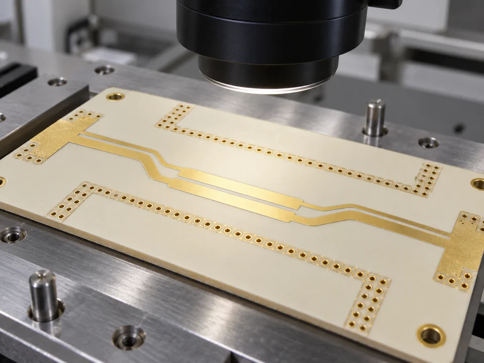
Check the artwork, conductor geometry, layer alignment, and accessible features through the production sequence.
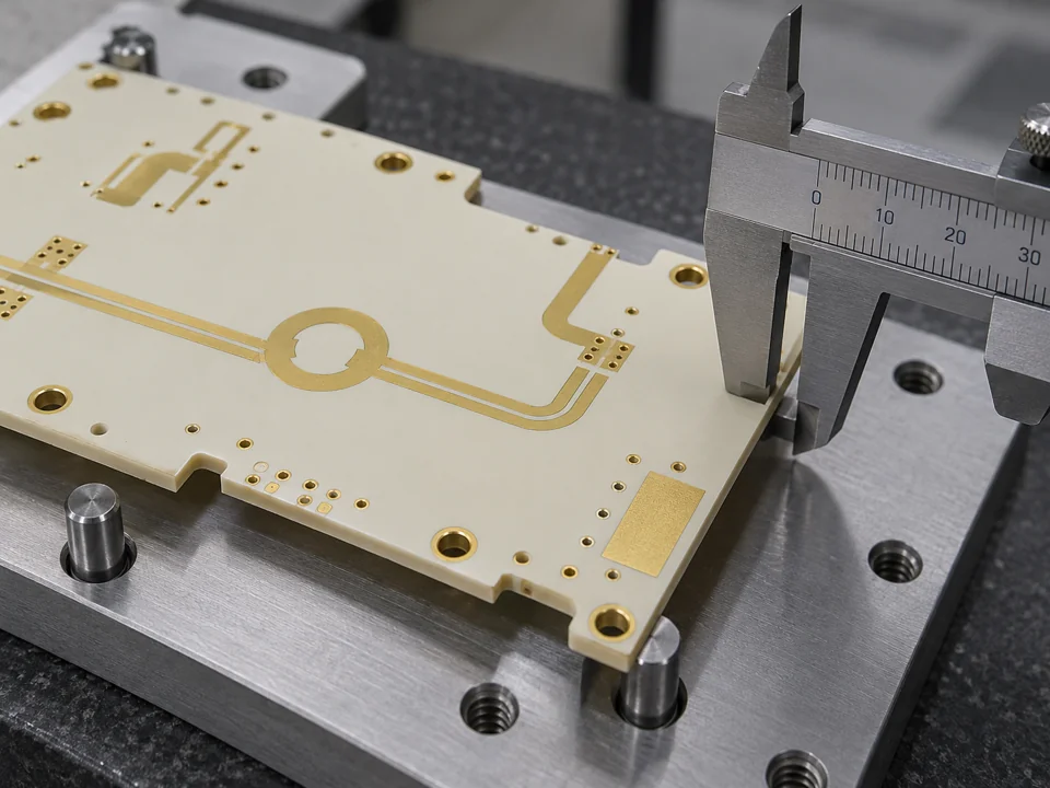
Review hole-wall quality, plated features, critical dimensions, and agreed sample or coupon checks.
Electrical test verifies connectivity and isolation. Impedance and application-specific RF measurements follow the separately agreed plan.
START YOUR PROJECT
Send your Gerber or agreed fabrication files, drill data, stack-up, exact laminate grades, copper requirements, quantities, and delivery target. Add impedance and RF test requirements; include the BOM and placement data for assembly.
Send Your Rogers PCB InquiryEmail: info@mv-circuit.com
COMMON QUESTIONS
It is a circuit board built using a specified Rogers Corporation laminate for part or all of its dielectric structure. Rogers is a material supplier; MV Circuit fabricates the board to the agreed design and construction.
No. RO4000 products use hydrocarbon/ceramic thermoset systems, while families such as RT/duroid 5870 and 5880 use reinforced PTFE. These materials require different selection and processing considerations.
They have different dielectric and loss data, and RO4350B includes flame-retardant characteristics relevant to some designs. Compare the current supplier data sheets, assembly conditions, compliance needs, and the actual RF geometry before selecting either grade.
Process Dk is tied to a defined material characterization and acceptance method. Design Dk is intended to support electrical design under its stated conditions. They should not be substituted without understanding the model, frequency, and test method.
A suitable hybrid stack-up can combine RF laminate with FR-4 layers, subject to bonding compatibility, expansion behavior, registration, and electrical requirements. Send a full layer-by-layer construction for review.
Frequency alone is not enough. Provide the loss budget, line length, dielectric thickness, Dk requirements, copper profile, thermal conditions, and geometry. Material selection should be checked against simulation and any required prototype measurements.
There is no single best option. Consider the signal geometry, conductor finish, soldering, contact wear, and storage requirements. Identify selective finish areas and ask for a review before releasing the drawing.
No. It evaluates the agreed transmission-line characteristic under the specified method. Insertion loss, return loss, radiation, and complete system behavior need their own defined measurements and acceptance criteria.
We support fabrication, component sourcing, SMT assembly, and agreed testing. Include the BOM, placement files, assembly drawing, sensitive RF components, and any programming or functional-test instructions with your inquiry.
Material grade and availability, layer count, hybrid bonding, copper structure, geometry, panel utilization, inspection, assembly, and quantity influence the quotation. The delivery schedule is confirmed after the data package and construction are reviewed.
CUSTOMER FEEDBACK
“Their attention to detail and commitment to delivering high-quality PCBs on time has helped streamline our production process. The team is highly responsive and always willing to provide expert advice.”
Michael S. · USA
Existing feedback about MV Circuit’s overall PCB service, not a Rogers-specific project endorsement. View the original feedback.
Rogers, RO4000, RT/duroid, and the relevant material names are trademarks of Rogers Corporation. Material references identify the specified laminate; they do not imply an affiliation or endorsement.