
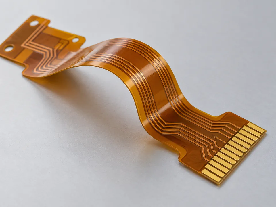
A flexible PCB is more than a thin circuit board that bends. Its conductor pattern, dielectric films, coverlay, interconnections, and local reinforcement must work together in the final assembly. A circuit that looks acceptable while flat can still fail if its construction does not suit the intended movement.
This guide explains a typical flexible PCB manufacturing route and the decisions that influence it. The exact sequence varies with the layer count, via structure, material system, and fabrication method; it is not one fixed recipe for every flex design.
How the Circuit Construction Changes the Process
The number of conductive layers determines which manufacturing steps are necessary. A single-sided flex tail does not need the same interconnection process as a multilayer flex circuit.
| Construction | Main manufacturing differences | What to define early |
|---|---|---|
| Single-sided flex | One patterned copper layer; interlayer plating is unnecessary unless special features require it. | Contact openings, conductor orientation, finished thickness, and reinforcement. |
| Double-sided flex | Two copper layers may be connected by plated holes; both sides require registration and protection. | Via locations, bend zones, plating needs, and coverlay openings. |
| Multilayer flex | Patterned inner layers are bonded into a stack, with interconnections processed to the specified structure. | Layer-by-layer stack-up, bonding materials, via pairs, and bending conditions. |
Rigid-flex PCBs add rigid regions and rigid-to-flex transitions. Their lamination and mechanical requirements need a separate review rather than being treated as a thicker version of an all-flex circuit.
1. Review the Design Before Releasing Production
Manufacturing starts with the data package. The engineering team compares the artwork, drill files, stack-up, mechanical drawing, and acceptance requirements. Missing information at this stage often creates more delay than a difficult fabrication feature.
For flex circuits, the drawing should identify the bend area, bend direction, final installed shape, and whether movement is occasional or repeated. The review also checks contact-pad access, stiffener boundaries, hole-to-copper clearances, and the relationship between coverlay openings and solderable lands.
- Electrical data: fabrication artwork, drill data, layer identification, and any impedance requirements.
- Mechanical data: outline, tolerances, folded drawing, connector requirements, and keep-out areas.
- Construction data: dielectric, copper, adhesive, coverlay, stiffeners, and finished thickness.
- Validation data: inspection criteria and any application-specific bend, thermal, or environmental testing.
The agreed construction should be recorded before tooling and material allocation. A generic minimum bend-radius ratio cannot replace this design-specific review.
2. Select and Prepare the Flexible Materials
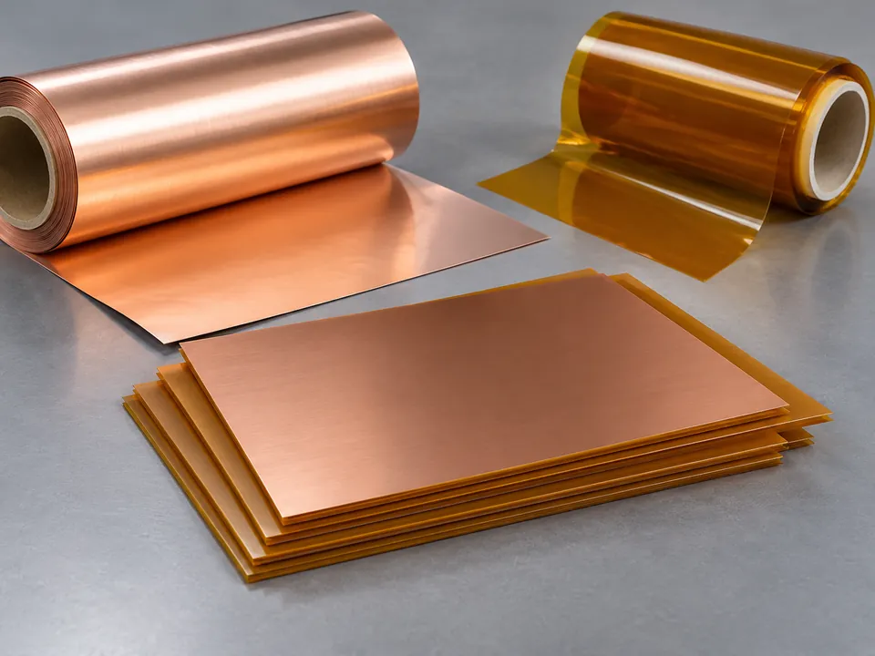
Many flex circuits begin with purchased flexible copper-clad laminate rather than a separate copper-lamination operation at the PCB factory. Polyimide is widely used where thermal resistance and dimensional performance are important. Polyester-based constructions also exist, but their processing and assembly compatibility must be assessed separately.
Adhesive-based laminates include a bonding layer between copper and dielectric. Adhesiveless systems remove that particular adhesive layer; they are still complete material systems with their own thicknesses and processing requirements. Copper foil type and thickness should be chosen for the electrical load, routing geometry, and intended flexing behavior.
Panels are cut and prepared with suitable support and registration features. Cleanliness, moisture management, and careful handling help prevent contamination, creases, and dimensional variation. Drying conditions follow the material supplier’s guidance and the qualified production process.
3. Form the Circuit Pattern by Imaging and Etching
Transfer the artwork to the copper
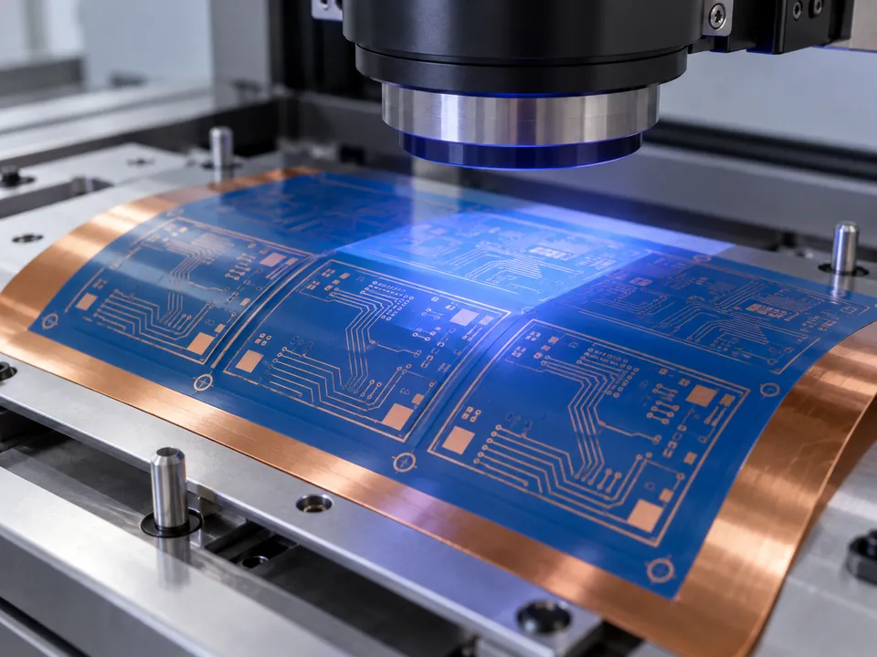
A photoresist layer is applied to the prepared copper surface. Imaging equipment transfers the circuit artwork into the resist, and development produces the required protective pattern. Registration is particularly important because thin flexible materials can move during processing.
The fabricator controls surface preparation, resist adhesion, exposure, and development so fine features remain intact. The artwork may include process compensation; the manufactured conductor dimensions must still meet the agreed drawing.
Remove unwanted copper
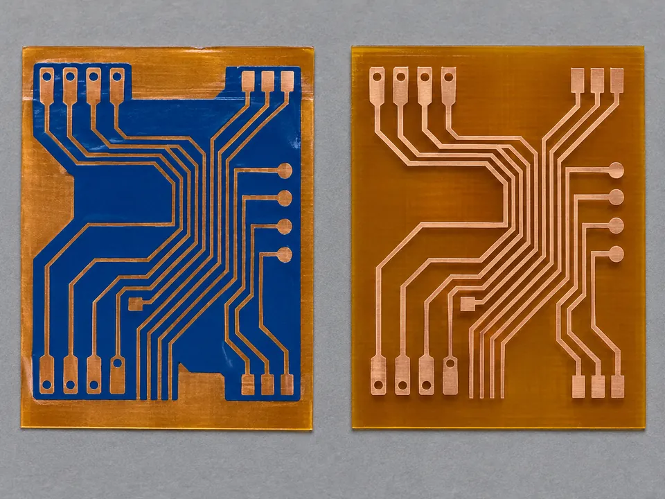
In a subtractive process, etching removes exposed copper and leaves the intended conductors. The resist is then stripped at the appropriate stage. Etchant condition, copper thickness, line geometry, and transport through the process influence the finished trace shape.
Over-etching can narrow conductors; incomplete etching can leave unwanted copper connections. Optical inspection checks the patterned layers for features such as opens, shorts, and damaged traces before later operations make them harder to inspect. Pattern-plating and other fabrication routes alter the detailed order of imaging, plating, and etching.
4. Drill and Metallize Interconnections Where Required
Double-sided and multilayer circuits commonly need connections between copper layers. Mechanical drilling or laser processing is selected according to the feature type and the approved construction. Not every flex circuit requires laser drilling, and not every hole is an electrical via.
For plated interconnections, hole preparation removes residues and conditions the hole walls for metallization. A conductive seed layer and subsequent copper plating establish the connection between the specified layers. Drill registration, hole-wall quality, and plating distribution all affect the result.
The finished copper in and around a hole changes the local mechanical behavior. Via placement therefore needs to be reviewed against the bend area, rather than assuming a plated connection can tolerate the same movement as a continuous thin conductor.
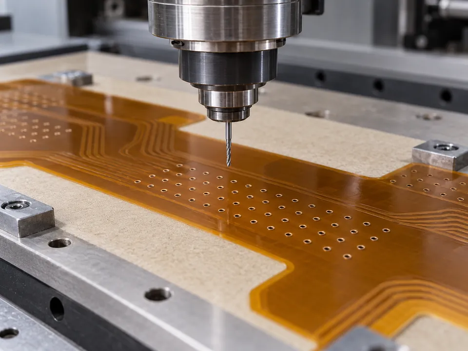
In multilayer production, some inner layers are imaged and inspected before stack lamination. Through-holes or other interconnections may then be drilled and plated. The manufacturer confirms the complete sequence for the particular layer structure.
5. Apply Coverlay and Complete the Required Bonding
Coverlay protects conductors while leaving selected pads accessible. A common construction uses polyimide film with an adhesive layer. Openings are prepared in the coverlay, aligned to the circuit, and bonded using a qualified lamination cycle. DuPont’s coverlay documentation describes its role as electrical insulation and environmental protection for etched circuitry.
The process must account for registration and adhesive movement. Too much adhesive intrusion can reduce usable pad area; poor bonding can leave voids or lifted edges. The opening shape, pad size, adhesive thickness, and local copper pattern are reviewed together.
Flexible solder masks are another option for appropriate constructions, particularly where fine openings are needed. Coverlay and solder mask are not automatically interchangeable: bend behavior, material compatibility, and the application determine suitability.
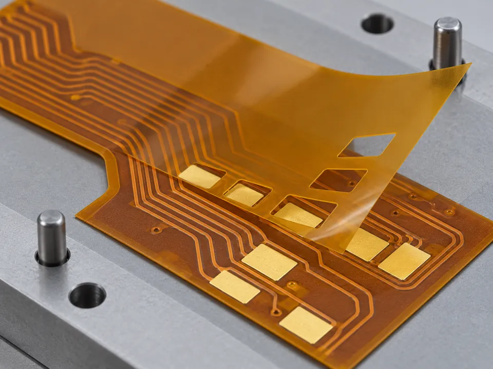
Multilayer circuits also require controlled bonding between layers. The pressure, temperature, time, and lay-up materials are process-specific. Values from one material family should not be copied into another construction without qualification.
6. Finish the Pads and Add Local Reinforcement
Protect exposed connection areas
Surface finish is applied to exposed copper according to the assembly or contact requirements. Options may include ENIG, immersion tin, OSP, or an appropriate plated gold system, subject to the approved process. A finish suitable for soldering is not necessarily the right choice for a repeated-mating connector contact.
The specification should identify which areas need finishing and any required coating thicknesses. Plating on a bend zone can change its mechanical behavior, so exposed contacts and flexible conductor areas should be considered separately.
Bond stiffeners where support is needed
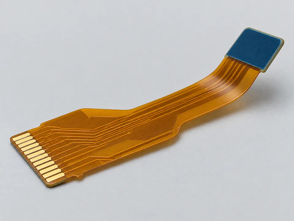
Stiffeners reinforce selected locations such as connector tails, component areas, or mounting points. Polyimide, FR-4, or metal reinforcement may be used when appropriate. A stiffener normally provides mechanical support; it does not turn an all-flex circuit into an electrically integrated rigid-flex PCB.
For connector tails, the complete thickness through the contact region matters, including the flex and reinforcement. Stiffener position, adhesive choice, edge geometry, and the transition into the flexible area must match the drawing.
7. Profile, Inspect, Test, and Protect the Finished Circuit
Cut the outline without damaging the flex
Laser cutting, punching, routing, or other suitable methods define the final outline and openings. Method selection depends on geometry, material thickness, tolerances, and production volume. Edge quality matters because nicks and sharp internal features can initiate tears during handling or installation.
Dimensional inspection checks critical outlines, hole positions, contact dimensions, and stiffener registration. The circuit must be supported during measurement so distortion is not mistaken for a dimensional error.
Verify the agreed electrical and visual requirements
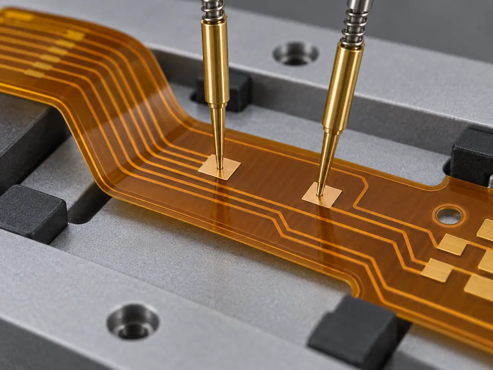
Electrical testing checks connectivity and isolation against the intended circuit. Visual inspection and AOI examine accessible features such as conductor patterns, coverlay alignment, exposed pads, contamination, and mechanical damage.
Microsections, impedance checks, thermal testing, or bend validation may be added when required by the design and acceptance plan. Passing a continuity test does not by itself establish repeated-flex life. Qualification should represent the actual construction, movement, and environment.
Prepare for assembly and shipment
Flexible circuits may need carriers or support tooling for SMT assembly. Handling and any moisture-control requirements should be agreed before delivery. Packaging protects the circuits against folding, creasing, abrasion, and contamination, with lot identification retained for traceability.
Common Defects and the Controls That Address Them
| Issue | Potential contributors | Useful control |
|---|---|---|
| Open or shorted traces | Imaging defects, etch variation, contamination, or handling damage. | Layer inspection and electrical test. |
| Misaligned coverlay | Registration variation, dimensional movement, or lay-up error. | Opening review and registration checks. |
| Delamination or voids | Moisture, contamination, incompatible materials, or an unsuitable bonding cycle. | Material control and qualified lamination. |
| Cracks near a bend | Unsuitable construction, local reinforcement, tight folding, or strain concentration. | Mechanical review and representative bend validation. |
| Poor connector fit | Incorrect total thickness, stiffener position, or contact geometry. | Drawing review and contact-region measurement. |
These are possible contributors, not a substitute for failure analysis. The correct action depends on where the defect occurs and the evidence from the affected circuit.
What to Send for a Flexible PCB Manufacturing Review
A complete inquiry helps the manufacturer review the electrical and mechanical requirements together:
- Gerber or other agreed fabrication data, drill files, and a revision-controlled drawing.
- Layer-by-layer stack-up, copper construction, coverlay, adhesive, and finished thickness.
- Bend location, installed geometry, movement expectations, and operating environment.
- Stiffener drawings, connector part requirements, pad finishes, and critical tolerances.
- Quantity, delivery target, acceptance criteria, and any qualification or test requirements.
- BOM and placement data if fabrication and assembly are required together.
Plan Your Flexible PCB with MV Circuit
Send your files and mechanical requirements for a manufacturing review. Our team can coordinate flexible PCB fabrication, component sourcing, assembly, and the agreed inspection scope.
Frequently Asked Questions
Is copper always laminated onto polyimide at the PCB factory?
No. Many production routes start with purchased copper-clad flexible laminate. Additional bonding or lamination may then be required for the final multilayer construction.
Does every flexible PCB need plated holes?
No. A simple single-sided circuit can connect its conductors without interlayer plating. Double-sided and multilayer constructions may require plated interconnections as defined by the design.
What is the difference between coverlay and a stiffener?
Coverlay insulates and protects the conductor pattern while exposing selected pads. A stiffener adds local mechanical support, for example under a connector tail. They perform different functions.
Can a finished flexible PCB bend repeatedly?
Only when its materials, geometry, and construction are designed and validated for the required movement. A flex-to-install circuit should not automatically be treated as a dynamic-flex design.
What determines manufacturing cost and delivery time?
Layer count, materials, panel utilization, fine features, interconnections, reinforcement, tooling, inspection, and order quantity all matter. Final timing follows engineering review and material availability checks.
Technical references: All Flex circuit design guide; DuPont Pyralux LF coverlay data sheet.
This is a general manufacturing guide. Product-specific limits and acceptance requirements are confirmed for the agreed construction.